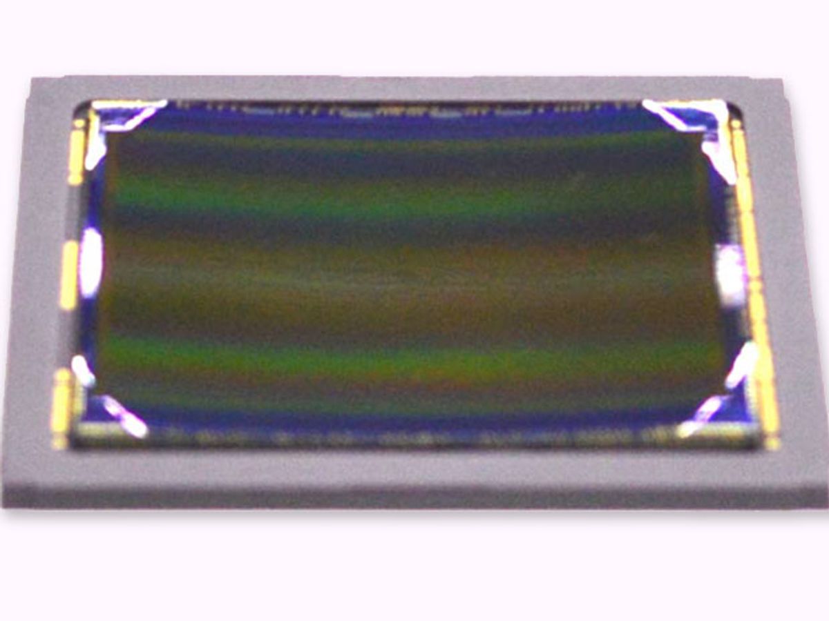
The retinas of humans and other animals line the curved inner surface of the eye. Now, in a bit of biomimicry, Sony engineers report that they have created a set of curved CMOS image sensors using a "bending machine" of their own construction.
The result is a simpler lens system and higher sensitivity, Kazuichiro Itonaga, a device manager with Sony's R&D Platform in Atsugi-shi, Japan reported on Tuesday at the Symposium on VLSI Technology in Honolulu, Hawaii.
A curved CMOS sensor has a few advantages over a planar sensor, Itonaga said. Because of the geometry, it can be paired with a flatter lens and a larger aperture, which lets in more light. Photodiodes at the periphery of a sensor array will be bent toward the center, which means light rays will hit them straight on instead of obliquely. What's more, the strain induced on a CMOS sensor by bending it alters the band gap of the silicon devices in the sensor region, lowering the noise created by "dark current" — the current that flows through a pixel even when it is receiving no external light.
All told, the curved systems were 1.4 times more sensitive at the center of the sensor and twice as sensitive at the edge, according to the Sony engineers.
Itonaga gave few details on the process the team used to create the curved CMOS chips. He said that a machine was used to bend the CMOS sensors and that they were backed with a ceramic to stabilize them after bending. It was also unclear how much the chips were curved, although Itonaga said that they did achieve the same level of curvature found in the human eye.
Two chips were reported. One, which measured some 43 millimeters along the diagonal, is a full-size chip for digital cameras. The other is a smaller chip, more suitable for mobile phones, which measured 11 mm along the diagonal and boasts smaller pixels. The team integrated the curved image sensor with a lensing system and showed an image that seemed to be quite good, although it wasn't displayed alongside an image taken with an equivalent flat sensor for comparison.
This isn't the first curved image sensor to be developed. In 2008, for example, John Rogers' group at the University of Illinois at Urbana-Champaign reported they'd made a curved photodetector array by bending an array of photodiode islands connected by compressible interconnect. But Sony's work might be a bit closer to mass manufacture. The team has made somewhere in the vicinity of 100 full-size sensors with their bending machine. "We are ready," Itonaga said.
Rachel Courtland, an unabashed astronomy aficionado, is a former senior associate editor at Spectrum. She now works in the editorial department at Nature. At Spectrum, she wrote about a variety of engineering efforts, including the quest for energy-producing fusion at the National Ignition Facility and the hunt for dark matter using an ultraquiet radio receiver. In 2014, she received a Neal Award for her feature on shrinking transistors and how the semiconductor industry talks about the challenge.


