Wonderful as silicon-based transistors are, they break down at temperatures above 350 °C. For higher-temperature environments, such as those found in jet engines and deep oil wells, researchers have had to turn to other options such as silicon carbide circuits, which can survive up to 550 °C.
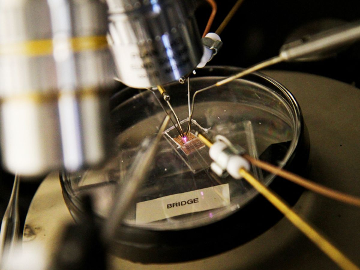
Now, researchers at the University of Utah have made tiny plasma-based transistors that work at the blistering temperatures found inside nuclear reactors. While plasma transistors were first reported five years ago, the new devices are 500 times smaller than those early versions.
The new micro-plasma transistors work at temperatures of up to 790 °C. They could be used to make electronics for controlling robots that conduct tasks inside a nuclear reactor, says Massood Tabib-Azar, the professor of electrical and computer engineering at the University of Utah who developed the devices. Such extreme-temperature logic circuits could also control nuclear reactors in case of emergencies or nuclear attacks. Tabib-Azar and his postdoctoral researcher, Pradeep Pai, reported the plasma transistors online today in the journal IEEE Electron Device Letters.
In a conventional three-terminal field-effect transistor, the voltage applied at the gate terminal controls the current flowing through a semiconductor channel. A voltage that is above a certain threshold turns the device on.
The channel in a plasma transistor consists of a partially ionized gas, or plasma, instead of a semiconductor. An electron emitter, typically silicon, injects electrons into the plasma when a voltage is applied to it. Plasmas are generated at very high temperatures, making them suitable for an extreme-environment transistor. Today’s plasma transistors, which are used in light sources and medical instruments, are about 500 micrometers long and operate at more than 300 volts, requiring special high-voltage sources.
The new devices are between 1 and 6 microns in length and operate at one-sixth the voltage. Tabib-Azar and Pai made the transistors by first depositing layers of a metal alloy to form the gate on a 10-centimeter glass wafer. They deposited a thin layer of silicon on top of the gate. Then they etched away portions of the silicon film using a chemically reactive gas, creating cavities and empty spaces that they could fill with the plasma to form the transistor's channel. They used helium as the plasma source.
The researchers are working on connecting the devices to make logic circuits that they plan to test in the experimental nuclear reactor at the University of Utah.
In addition to working in nuclear reactors, the new extreme-temperature transistors could be used to generate X-rays. Instead of using bulky lenses and X-ray shaping devices, engineers could use these tiny devices to pattern microscale devices in silicon. Or this type of transistor could be incorporated in a smartphone, creating an X-ray imaging source to collect images of wounded soldiers in the battlefield, says Tabib-Azar.
Photo: Dan Hixson/University of Utah
Prachi Patel is a freelance journalist based in Pittsburgh. She writes about energy, biotechnology, materials science, nanotechnology, and computing.


