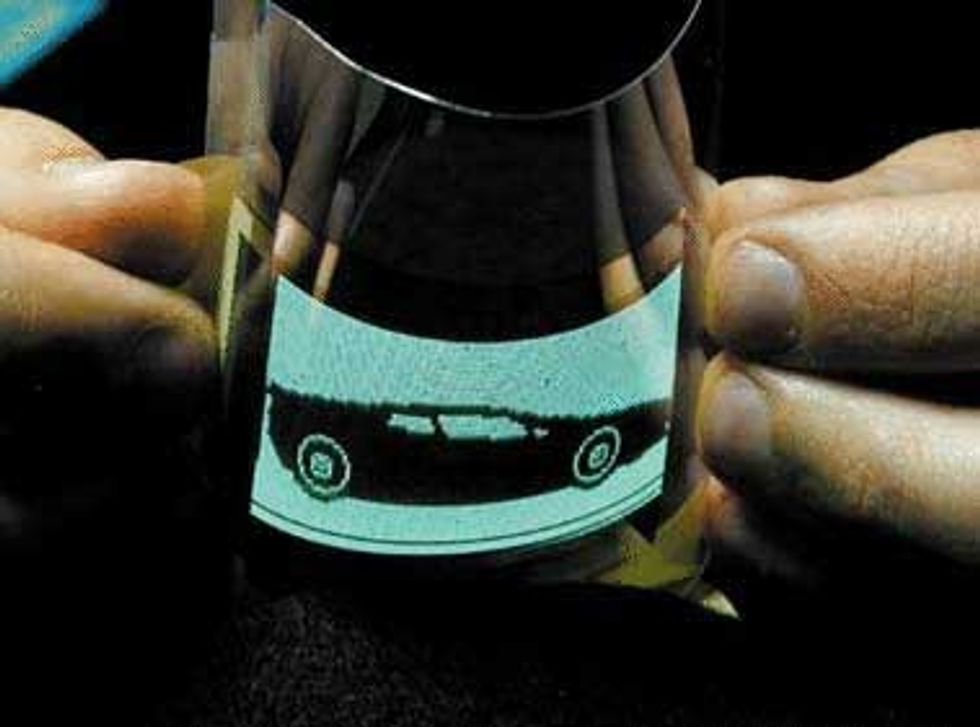
Organic Materials Are Poised As Never Before To Transform the world of circuit and display technology. Major electronics firms such as Philips and Pioneer, and smaller companies such as Cambridge Display Technology, Universal Display, and Uniax, are betting that the future holds tremendous opportunity for the low cost and sometimes surprisingly high performance offered by organic electronic and optoelectronic devices. Using organic light-emitting devices (OLEDs), organic full-color displays may eventually replace liquid-crystal displays (LCDs) for use with laptop and even desktop computers. Such displays can be deposited on flexible plastic foils [Fig. 1], eliminating the fragile and heavy glass substrates used in LCDs, and can emit bright light without the pronounced directionality inherent in LCD viewing, all with efficiencies higher than can be obtained with incandescent light bulbs.
[1]
An organic passive-matrix display on a substrate of polyethylene terephthalate, a lightweight plastic, will bend around a diameter of less than a centimeter. The 18-mm-thick, 5-by-10-cm monochrome display consists of 128 by 64 pixels, each measuring 400 by 500 µm, and is being operated at conventional video brightness of 100 cd/m2. It was fabricated by Universal Display Corp., Ewing, N.J., with a moisture barrier built into the plastic that prevents degradation of the pixels.
Organic electronics are already entering the commercial world. Multicolor automobile stereo displays are now available from Pioneer Corp., of Tokyo, and Royal Philips Electronics NV, Amsterdam, is gearing up to produce both OLED backlights to be used in LCDs and organic integrated circuits. It is possible that soon, portable and lightweight roll-up OLED displays will cover our walls, replacing the bulky and power-hungry cathode ray tube that has been the television standard for 50 years.
Given the need for very low-cost (but not always high-performance) circuits for everything from smart cards carrying personal information, to building entry cards, to inventory control, it is reasonable to assume that within 10 years, the square footage of organic circuitry might exceed that of silicon electronics (though one expects that silicon transistors would still vastly outnumber and outperform those fabricated from organic materials.)
Organic semiconductors have been the subjects of intense scientific investigation for the past 50 years. During most of that time, these materials, primarily consisting of carbon, hydrogen and oxygen, were considered to be merely a scientific curiosity. Organic materials' weak intermolecular bonds in the solid state give them properties of both semiconductors and insulators; so their study has deepened our fundamental understanding of the electronic and optical properties of solids. But, organic semiconductors attracted industrial interest when it was recognized that many of them are photoconductive under visible light. This discovery led to their use in electrophotography (or xerography) and as light valves in LCDs. There were even hopes that very low-cost thin-film solar cells and superconductors could be made using such substances.
Unfortunately, the potential of active electronic devices such as solar cells, light emitters, and thin-film transistors remained unfulfilled for decades because organic materials have often proved to be unstable. Further, making reliable electrical contacts to organic thin films is difficult, and when exposed to air, water, or ultraviolet light, their electronic properties can degrade rapidly. Finally, the low carrier mobilities characteristic of organic materials obviates their use in high-frequency (greater than 10 MHz) applications. These shortcomings are compounded by the difficulty of both purifying and doping the materials.
But in 1987 Ching Tang and Steven Van Slyke of Eastman Kodak Co., Rochester, N.Y., successfully addressed many of these problems when they produced the first efficient light emission from a two-layer organic structure resembling a pn junction. The Kodak group used a class of synthetic dyes that is closely related to well-understood xerographic materials to develop a device called a small-molecule OLED that produced light with about 1 percent efficiency. The materials used consist of often no more than 30 or 40 atoms covalently bonded into stable, individual molecular units, called monomers.
While this first demonstration of reasonably efficient light emission at low voltage attracted interest from potential display manufacturers, particularly in Japan, the technology attracted public attention when, in 1990, researchers at Cambridge University in England under the direction of Richard Friend reported a similar effect in a semiconducting organic polymer film consisting of poly para-(phenylene vinylene), or PPV. Unlike small molecule compounds, polymers are long chain molecules whose monomer segments are attached in a continuous covalently bonded, high-molecular- weight chain. Polymers tend to be environmentally rugged and flexible although, like small molecules, their electronic properties can rapidly degrade when exposed to oxygen or water.
Let There Be Light
Both polymeric and small molecule OLEDs [Fig. 2] operate by accepting charge carriers of opposite polarities, electrons and holes, from the cathode and anode contacts, respectively. An externally applied voltage drives these carriers into the recombination region where they form a neutral bound state, or exciton. There are two types of excitons formed, called singlets and triplets. On average one singlet and three triplets are formed for each four electron-hole pairs injected into the exciton formation region of the OLED.
Quantum mechanics allows de-excitation (or recombination) of the singlet within a few nanoseconds of formation. This leads to a photon emission and is called fluorescence. Recombination of the triplet exciton is slow (taking about 1 ms to 1 second) and when it does occur, usually results in heat rather than light. But If a heavy- metal atom such as iridium or platinum is placed in an otherwise organic molecule, the characteristics of singlet and triplet excitons mix, speeding the emission of light to within 100 ns-100 µs. This kind of emission is called phosphorescence.
Recent advances in boosting the efficiency of OLED light emission have led to the possibility that OLEDs will find early uses in many battery-powered electronic appliances such as cell phones, gameboys, and personal digital assistants. Typical external quantum efficiencies of OLEDs (defined as the ratio of the number of emitted photons to the number of injected electrons) made using a single fluorescent material that both conducts electrons and radiates photons are greater than 1 percent.
But by using guest-host organic materials systems where the radiative guest fluorescent or phosphorescent dye molecule is doped at low concentration (typically between 0.5 and 5 percent) into a conducting molecular host thin film, the efficiency can be substantially increased to 10 percent or higher for phosphorescence or up to approximately 3 percent for fluorescence.
Currently, efficiencies of the best doped polymer and molecular OLEDs exceed that of incandescent light bulbs. Efficiencies of 20 lumens per watt have been reported for yellow-green-emitting polymer devices, and 40 lm/W attained for phosphorescent molecular OLEDs, compared to less than 20 lm/W for a typical incandescent light bulb. It is reasonable to predict that soon, efficiencies of 80 lm/W--a value comparable to that of fluorescent room lighting--will be achieved using phosphorescent OLEDs.
A fundamental difference between small -molecule and polymeric devices is the manner in which they are constructed. Small molecules are deposited in thin layers around 5-100 nm by high-vacuum thermal sublimation. That technique heats powder sources of the molecules in a vacuum to a temperature high enough to evaporate, but low enough to avoid their decomposition (about 250 o to 450 oC). The evaporated molecules then collect on a cool substrate to form a film whose thickness can be precisely controlled to near monolayer accuracy.
Small-molecule OLEDs are grown on a glass or plastic substrate to form a multi-layer structure about 100 nm thick [Fig. 2]. The substrate is first coated with a conducting transparent electrode such as indium tin oxide (ITO) or polyaniline, which serves as the anode. This is followed by a thin, hole-transporting organic layer (HTL) typically made from chemicals called diamines. An organic light-emitting layer of comparable thickness is then deposited onto the HTL surface. This latter stratum often doubles as the electron-transporting layer (ETL). Finally, the device is completed by depositing a cathode consisting of a metal with a low work function such as calcium or an alloy such as magnesium-silver onto the ETL surface. A low work function is necessary to ensure efficient, low-resistance injection of electrons from the cathode into the ETL.
Changing the composition of the layers tunes the OLED emission colors across the visible spectrum. Green emission can be achieved by doping an electron-conducting organic matrix called Alq 3 with either a small amount of an iridium phosphor or fluorescent dyes. The pigment perylene when doped into an ETL known as CBP emits blue light. Lanthanide complexes and porphyrin pigments have been used to efficiently emit red light when doped into Alq 3 or CBP.
Researchers have encountered many difficulties in manufacturing devices with the thin layers needed to achieve operating voltages between 5 V and 10 V. OLEDs are vulnerable to shorts caused by pinhole defects in the film or contamination of the substrate surface by dust particles. Furthermore, the materials tend to be mechanically fragile and are easily attacked by chemicals used in photolithographic patterning. Therefore, patterning often requires low-resolution methods, such as defining the device contact by metal deposition through a shadow mask, often in combination with costly dry- processing techniques. In the future, however, many new nanolithographic patterning techniques will appear and even techniques borrowed from other industries such as injection molding, direct imprinting using stamping, and ink jet printing.
The most efficient polymer-based devices use bilayer structures similar to molecular organic devices or blends of electron- and hole-transporting materials. In contrast to vacuum-grown small-molecule OLEDs, polymers, or their precursors are typically cast as a liquid onto indium-tin-oxide-coated substrates. Then, once the film has been thinned by spinning the substrate or other methods, it is solidified by heating. While the application of the organic layers occurs by such potentially low-cost wet-chemistry processes, a low-work-function metal cathode must still be vacuum deposited.
Polymer OLED structures can be simpler than small-molecule structures. The first polymer layer (in contact with ITO) can serve solely as a hole-injecting/conducting layer; in some cases a single layer is used for electron and hole injection, conduction, and light emission. Polymer OLEDs also often operate at lower power than small-molecule devices. Due to their high conductivity, polymer-based devices have operating voltages in the 2-5-V range, which is 1-2 V lower than small-molecule OLEDs.
Control of film composition and thickness uniformity to dimensions required in single- and double-layer OLEDs is straightforward by vapor deposition but problematic by spin-on techniques. Since polymers are cast from solution, care must be taken in multilayer structures to ensure that the solvent used for the second layer does not dissolve the first. Hence, chemical compatibility between successively applied polymers ultimately limits the complexity of the device structures fabricated using these materials.
As in small-molecule devices, changing the chemistry of the polymer can tune the color of an OLED. For example, adding electron-donating groups to the PPV chain red-shifts its light emission to orange. Conversely, adding electron-acceptor groups gives a blue shift. Similar shifts are obtained in the Alq 3 system by adding methyl groups to a particular chemical structure. However, even such simple chemical substitutions can change the device efficiency and reliability in an unpredictable manner.
And Full-Color Displays
One of the principal reasons that OLED technology has attracted such intense interest is its potential for use in full-color displays that might eventually replace active- matrix LCDs. A display consists of a matrix of contacts made to the bottom and top surfaces of each organic light-emitting element, or pixel [see sidebar, "Organic displays"]. To generate a full-color image, it is necessary to vary the relative intensities of three closely spaced, independently addressed pixels, each emitting one of the three primary colors of red, green, or blue.
[3]
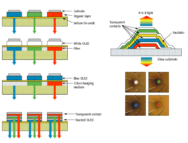
Several schemes exist for generating full color. The simplest is to place red, green, and blue (R, G, and B) pixels side by side and address them separately as in the top left diagram. Another way is to use a single white-emitting organic LED (OLED) and filter its light through R, G, or B media or dielectric stacks [next image down]. Alternatively, a single, blue-emitting OLED may serve as a pump of R and G fluorescent color-changing media [third image, left]. Also, R, G, and B pixels may be stacked with intervening transparent contacts to form compact stacked OLEDs (SOLEDs) [bottom, left].
A stacked OLED was built at Princeton University with separate red, green, and blue subpixels in a vertical, coaxially emitting geometry [just below]. Because of the transparent contact layers, light is emitted from both the top and bottom of the device. Single pixels can be tuned to red, green, blue and white [bottom].
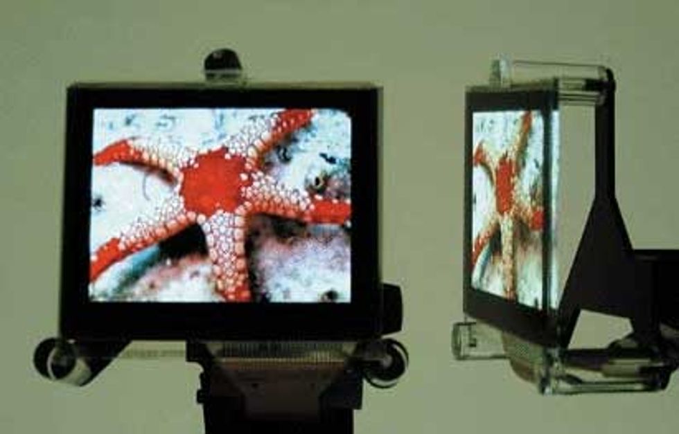
Several different techniques have been proposed for producing the three colors needed in each pixel [Fig. 3]. One method involves photolithographic patterning of the transparent indium-tin-oxide anode column electrodes on the substrate combined with deposition of metal through a mask to form the cathode row electrodes of the side-by-side-positioned red, green, and blue (R, G, B) subpixels, as shown at the top left of the figure. This approach, while architecturally obvious, requires a costly process where each of the three closely spaced color segments must be sequentially grown and patterned. In spite of this difficulty, Sanyo Electric Co. of Osaka, Japan, and Kodak recently demonstrated a prototype side-by-side molecular OLED flat panel [Fig. 4].
[4]
Eastman Kodak and Sanyo Electric developed this active-matrix, full-color organic display, only 1.8 mm thick, for digital still and video cameras and other portable imaging products. With a 2.4-inch diagonal screen and integrated drive electronics, the bright display has 852 by 222 pixels, a contrast ratio of more than 250:1, and a peak luminance of 200 cd/m2.
Alternatively, optical filtering of white OLEDs can produce acceptable red, green, and blue emission, as seen in the next diagram down in [Fig 3]. But this method sacrifices efficiency due to the large amount of light absorbed in the filters. Less efficiency is lost by using a single blue or ultraviolet OLED to pump organic fluorescent wavelength down-converters, also known as color-changing media (CCM), as illustrated in the third diagram on the left of [Fig 3]. Each CCM filter consists of a material that efficiently absorbs the blue light and re-emits the energy as either green or red light, depending on the compound used.
Organic thin films allow for the realization of completely new display architectures, which, among other advantages, may lead to the practical realization of low-cost, very high-resolution, full-color displays. For example, Vladimir Bulovic and co-workers at Princeton University in New Jersey demonstrated transparent OLEDs (or TOLEDs), that could be used in either transparent head-up, or high-contrast displays.
In addition to being a transparent light emitter, the top indium-tin-oxide surface of the TOLED can serve as the hole- injecting electrode for a second TOLED built on top of the first device, as shown in the bottom left diagram of [Fig. 3]. Each device in the stack is then independently addressable and can be tailored to emit its own color through the adjacent transparent organic layers, the transparent contacts, and the glass substrate. This allows the entire area of the vertically stacked pixel to emit any mixture of the three primary colors.
Recently the authors' laboratory constructed a full-color, transparent stacked OLED (SOLED) of the configuration shown in the bottom left diagram of [Fig. 3]. Because each color element in the stack is independently addressable, a SOLED display can be built with independent control of brightness, color, and gray scale. Although somewhat complex layering schemes are required, the structure is more compact than the side-by-side placement of red, green, and blue subpixel elements currently employed in cathode-ray tubes and LCDs, allowing for higher- resolution images.
One problem encountered with stacking numerous transparent organic layers is the formation of unwanted optical cavities whose resonances alter the emission spectra of OLEDs. While such effects are often undesirable and can be eliminated by careful control of layer thickness and composition, some researchers have suggested that multi-color displays can consist of OLEDs tuned by deliberately created cavities made from dielectric reflecting layers used in place of simple color filters.
The challenge to making full-color polymer-based displays is very different from that for making such displays using small- molecule OLEDs. Solution chemistry makes it difficult to deposit and pattern a polymer pixel of one color, and then repeat the process using a second color emitter because the solvents employed may dissolve or attack the devices already on the substrate.
Several schemes have been suggested to dodge this problem. One particularly promising method involves depositing a single blue-emitting polymer, and then selectively diffusing green and red dyes into adjacent regions. However, it has proved difficult to keep the diffusing dyes from bleeding into regions nearby. Seiko-Epson Corp. of Nagano, Japan, and Cambridge Display Technology Ltd., Cambridge, England, are pursuing a second approach in which the various polymer constituents of a full-color display are locally deposited using ink-jet printing. Here, control of the thickness and shape of the droplet, which eventually sets into a high-resolution pixel, remains an as-yet-unsolved problem.
Even if these solutions become practical, the fact remains that polymer OLEDs made with currently available materials have a broad-spectrum color emission. This raises additional barriers to realizing full-color displays. These difficulties have led companies such as Philips to develop early polymer OLED products primarily for highly uniform monochrome displays and backlights for LCDs.
Developing reliable organic devices remains a challenge. Charge conduction in these essentially insulating materials requires very high electric fields (1-5 MV/cm) so it is only the extreme thinness of OLEDs that enables them to operate at relatively low voltages. That thinness, coupled with a reactive top electrode, which is required to ensure efficient injection of electrons into the organic thin film, can contribute to rapid device degradation through the generation and subsequent growth of dark spots. The problem becomes especially acute when the devices are exposed to the atmosphere, which allows oxygen and other contaminants to react with the device layers. Only a few hours in air is enough to cause significant degradation through dark spot formation. However, even simple encapsulation in an inert atmosphere can greatly extend the useful device operating lifetime to well over 20 000 hours.
Ultimately, organic displays will only be as reliable as their constituent organic materials are stable. One recently demonstrated means to extend the lifetime of the devices is through the use of organic phosphors. The key to this approach is to reduce the amount of time a light-emitting molecule remains in the excited state. An excited molecule tends to be more reactive than the same molecule in its ground state, and the longer it remains excited, the more likely it is to degrade. Triplet excited states can live for periods approaching 1 second after formation. But introducing luminescent phosphor dopant molecules, as described earlier, can decrease triplet lifetime to a few hundred nanoseconds, thereby reducing the likelihood they will do damage. Using phosphor emitters, OLEDs have the potential to achieve operational lifetimes of many hundreds of thousands of hours, easily meeting all foreseeable demands on display performance.
The challenges researchers face in developing OLED devices are worth the reward. Because they can be printed on flexible surfaces such as polyester, organic light- emitters offer the potential for new types of displays and alternative methods of mass-production. Flexible, vacuum-deposited, molecular OLEDs have been demonstrated on ITO-coated polyester substrates and other polymers, opening up the possibility of roll-up or conformal displays on curved surfaces [again, Fig. 1]. Vacuum deposition onto plastic sheets also allows mass production of large-area OLEDs via roll-to-roll processing, where organic materials comprising the displays are continuously deposited on a flexible substrate translated between two reels. The successful development of such a process could result in low-cost manufacture of displays.
Organic Transistors
Organic semiconductors are also being applied to thin-film transistors. Developers hope to see them used for simple but information-packed product labeling and smart cards as well as in LCD and OLED back panels where large-area, low-cost active matrix transistor arrays are required. As in the case of OLEDs, organic thin-film transistors (OTFTs) and circuits have been investigated for many years, but only recently has their performance been sufficient to attract serious attention from the electronics community.
[5]
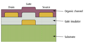
Inventor Corliss Organic thin-film transistors (OTFTs) are constructed of an organic or inorganic gate insulator and an organic semiconducting channel linking the source and drain..
Organic thin-film transistors [Fig. 5] can contain either a molecular or polymeric channel connecting the source and drain contacts. The gate electrode is first deposited onto an insulating substrate such as glass or plastic, followed by deposition of the gate insulator, which can consist of either an organic or inorganic dielectric film. Source and drain electrodes are deposited onto the gate dielectric, and that step is followed by the deposition of the thin-film channel layer. Since almost all patterning is done prior to the deposition of the organic material, standard photolithographic techniques can be employed to result in gate lengths of 5-m or less. Alternative methods such as injection molding or direct printing have also been successfully employed to generate potentially very low-cost circuits.
The performance of OTFTs is primarily limited by the low electron or hole mobilities of the channel materials. Due to molecular vibrations and large intermolecular distances (typically about 0.35 nm), conductivity in small-molecule organic films is determined by the rate of electron or hole hopping between organic molecules in the channel. Most probably, the mobility of organic films will not far exceed about 1 cm2/V-s at room temperature, which is low, but about equal to that of amorphous silicon already in use in display backplanes. Polymers tend to be less ordered than small molecules, leading to a mobility limit of perhaps two orders of magnitude smaller than that of small-molecule films.
OTFT circuits such as those recently reported by Philips, Lucent Technologies, and Pennsylvania State University, indicate the rapid advances that are currently being made in this very young field. The Philips group has fabricated a 15-bit programmable code generator consisting of 326 polymer OTFTs with 2-µm gate lengths. The interconnections between transistors are also conducting polymers. Interconnection between the conductors and the transistors was made by vias formed by an array of pins used to penetrate between layers, intermixing the conducting regions of the interconnects and the transistor contacts.
The channel mobility for these particular transistors was only 3 x10⁻⁴cm2/V-s. This, plus the time constant of the organic load transistors, resulted in a circuit operating frequency of less than 200 Hz. While the performance of this circuit is poor compared to inorganic electronic circuits, this level of integration at such an early stage of development is nevertheless encouraging. OTFT circuits will one day find applications where cost issues are more important than device speed.
The Organic Future
The first products using organic displays are already being introduced into the marketplace. And while it is always difficult to predict when and what future products will be introduced, many manufacturers are now working to introduce cell phones and personal digital assistants with OLED displays within the next one or two years. The ultimate goal of using high-efficiency, phosphorescent, flexible OLED displays in laptop computers and even for home video applications may be no more than a few years into the future.
However, there remains much to be done if organics are to establish a foothold in the display market. Achieving higher efficiencies, lower operating voltages, and longer device lifetimes are all challenges still to be met. But, given the aggressive worldwide efforts in this area, emissive organic thin films have an excellent chance of becoming the technology of choice for the next generation of high-resolution, high-efficiency flat-panel displays.
In addition to displays, there are many other opportunities for application of organic thin-film semiconductors, but to date these have remained largely untapped. Recent results in organic thin-film transistors provide the best example of an emerging organic electronic technology that may soon find commercial outlets in display backplanes and other low-cost electronics.
About The Author
Stephen Forrest F) has since 1997 served as the chair of the department of electrical engineering at Princeton University in New Jersey. He joined the Princeton Materials Institute and Princeton University In 1992 as the James S. McDonnell Distinguished University Professor of Electrical Engineering , and as director of Princeton's Center for Photonics and Optoelectronic Materials. Earlier, he obtained a Ph. D. from the University of Michigan in 1979. From there he went to Bell Laboratories in Murray Hill, N.J., and then to the University of Southern California, where he continued his reseach on semiconductor and organic optoelectronics. He has served on the Lasers and Electro-Optics Society (LEOS) Board of Governors, was an IEEE/LEOS Distinguished Lecturer in 1997, and in 1999 received the Materials Research Society (MRS) Medal. He is a member of the American Physical Society and MRS, and is a Fellow of the Optical Society of America.
Paul Burrows is currently with the Pacific Northwest National Laboratories in Richland, Wash. He graduated in 1989 from Queen Mary College, London, with a Ph.D. in physics. He has held post-doctoral appointments at the Riken Institute in Japan (1990-91) and at the University of Southern California (1992-93), and was a research scholar in the department of electrical engineering at Princeton from 1995 to 2000. Burrows chaired the IEEE/LEOS Technical Subcommittee on Displays from 1997-99.
Mark Thompson has been an associate professor in the chemistry department of the University of Southern California since June 1995. He was previously an assistant professor in the chemistry department at Princeton. He graduated from the California Institute of Technology with a Ph.D. in chemistry in 1985. He then took a Science and Engineering Research Council postdoctoral fellowship with the Inorganic Chemistry Laboratory in Oxford, England.
To Probe Further
The first demonstrations of organic light-emitting devices are described in two classic papers: "Organic Electroluminescent Diodes," by C. W. Tang and S. A. Van Slyke, Applied Physics Letters, Vol. 51, pp. 913-915 (1987); and "Light Emitting Diodes Based on Conjugated Polymers," by J. H. Burroughes, et al., in Nature, Vol. 347, pp. 539-541 (1990).
A recent review of the status of OLED technology can be found in "Prospects and Applications for Organic Light Emitting Devices," by P.E. Burrows, S.R. Forrest, and M.E. Thompson in Current Opinion in Solid State and Materials Science, Vol. 2, pp. 236-243 (1997). Also, a general overview of many of the challenges and opportunities relating to small-molecule organic materials and devices can be found in "Ultrathin Organic Films Grown by Organic Molecular Beam Deposition and Related Techniques," by S.R. Forrest, Chemical Reviews, Vol. 97, pp. 1793-1896 (1997).
For a complete compendium of the properties of organic materials, refer to Electronic Properties in Organic Crystals and Polymers, M. Pope and C. E. Swenberg, second edition (Oxford, 1999).
Finally, for those interested in some of the results discussed in the article, see "High Efficiency Phosphorescence from Organic Electroluminescent Devices," by M.A. Baldo, et al., Nature, Vol. 395, pp. 151-154 (1998); "Operating lifetime of phosphorescent organic light emitting devices," P.E. Burrows, S.R. Forrest, T. X. Zhou, and L. Michalski, Applied Physics Letters, Vol. 76, pp. 2493-2495 (2000); "Low Cost All-Polymer Integrated Circuits," by C. J. Drury, et al., Applied Physics Letters, Vol. 73, pp. 108-110 (1998); and "A Full-Color Transparent Metal-Free Stacked Organic Light Emitting Device with Simplified Biasing," by G. Parthasarathy, et al., in Advanced Materials, Vol. 11, pp. 907-910 (1999).