
Can any electronics material rival silicon—tunable, current-carrying, self-insulating, easy to fabricate, as common as sand on the beach? Even if another rival came forward, could it ever overcome silicon’s 50-year, trillion-dollar head start in development?
Yet we do need an adjunct to silicon, because so much of the potential market for electronics has yet to be opened. Electronics in paper, on walls, and in clothing are today mere novelties, simply because silicon can’t easily be painted on a surface, draped on a flexible platform, or used to cover large areas. What’s needed is something that can do all that and still be churned out cheaply and in bulk, processed easily, and slipped deftly into the guts of the next generations of electronics.
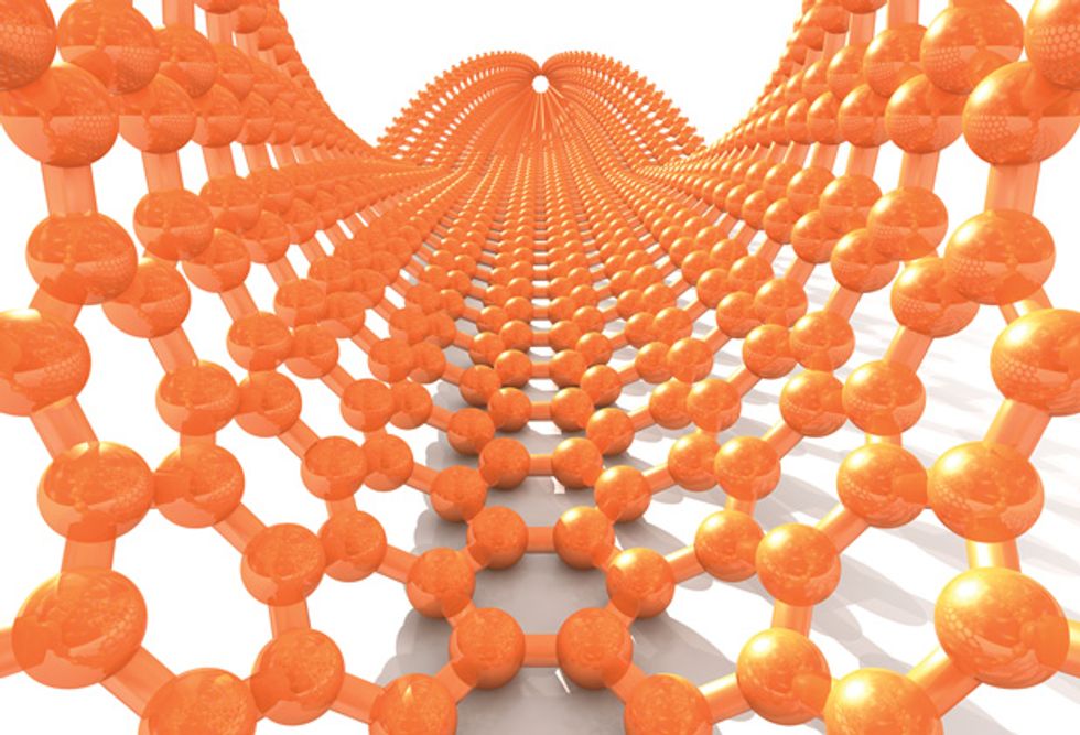
Allow us to suggest a candidate: graphene, an atom-thick sheet of carbon linked in a hexagonal network, like chicken wire. The material isn’t so much a replacement for silicon as a complement to it, serving many purposes where silicon is inadequate and mixing with silicon in the fabrication of certain devices. Graphene was discovered in the 1970s but first properly appreciated only in 2004, when Andre Geim and Konstantin Novoselov, Russian-born researchers at the University of Manchester, in England, managed to transfer it to a substrate and study its unique attributes. That work has won them the 2010 Nobel Prize in Physics.
Of course, any new form of pure carbon would be big news, but graphene’s properties are remarkable. As thin in one of its dimensions as a material can get, it is nevertheless impermeable to gas and is the strongest two-dimensional material ever tested, with a tensile strength 200 times as great as that of steel. What’s more, it conducts heat better than any metal. Best of all—to readers of this magazine—are graphene’s unusual electrical characteristics, especially its ability to carry charge carriers at speeds dwarfing those possible in silicon. That ability could allow for superfast switching in data processing.
Silicon has seen many a contender in the past—for instance, germanium, the material used for the very first transistor, and gallium arsenide, which for all its usefulness remains a mere niche material. So why do we nurse such high hopes for this rarefied form of carbon?
First, recall that carbon stands just above silicon in the periodic table, and hence shares many of silicon’s inherent properties. Second, consider that researchers around the world are rapidly accumulating new knowledge of graphene’s fantastic properties and getting better by the month at manufacturing it in bulk. Finally, keep in mind that the semiconductor manufacturing industry is under increasing stress to keep pace with Moore’s Law, and therefore more likely to consider new materials.
So the question really isn’t “Why graphene now?” but rather: “Why didn’t the electronics industry start with graphene in the first place?”
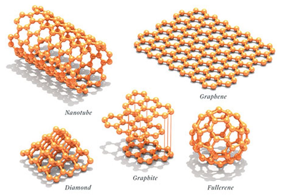
To appreciate this wonderful stuff, you have to put it in its context as one of the handful of forms that pure carbon can assume. There’s diamond, a three-dimensional crystal. There are the hollow cage molecules of fullerene, which are nearly dimensionless dots, and the related carbon nanotubes, whose length is so much greater than their width that they’re essentially one dimensional. And then there’s boring old graphite, made up of stacks of two-dimensional graphene sheets, mined or produced synthetically in the hundreds of thousands of tons and used in electrodes, lubricants, carbon-fiber-reinforced plastics, and pencil lead. The distinction between graphite and graphene is somewhat arbitrary; current thinking holds that more than 10 stacked sheets of graphene qualifies as graphite, and anything less is graphene.
Interestingly, graphite behaves differently in one direction than it does in another. The atoms in a given layer grip one another with strong carbon-carbon bonds, the same kind that give diamond its hardness. These links are only about 0.14 nanometer long. However, the layers are about 2.5 times farther apart, so the attractive forces in those directions are weaker. The layers can therefore easily slide across one another; the friction of a pencil passing across a sheet of paper is enough to shear off graphene sheets. We’ve been writing with graphene for centuries without appreciating it.
For decades, researchers thought (with some theoretical basis) that graphene could not exist in a freestanding form but only as a component—stacked into graphite, rolled into nanotubes, or balled into fullerenes. As often happens, the theorists were proven wrong by experimentalists.
Before that great discovery in 2004, some researchers had actually created graphene by laying hydrocarbons down on metal surfaces through chemical vapor deposition (CVD). But nobody paid much attention to these results, because the researchers had never bothered to transfer the graphene films onto insulating substrates, where the films might have been probed electronically.
Astonishingly, in the 21st century, when groundbreaking scientific discoveries are supposed to require sophisticated research tools, these first graphene flakes were “fabricated” simply by peeling them from a graphite crystal using adhesive tape. These first graphene samples were then subjected to tests of their strength, thermal conductivity, and electrical behaviors. Even after six years of intense research, graphene continues to reveal new and stellar properties.
The most striking property of graphene is the speed with which it can convey charged particles, the medium for information in all electronic systems. Even at room temperature, electrons and holes—positively charged entities that each represent the absence of an electron—can zip through graphene ballistically, traveling for micrometers at a stretch without bouncing off a carbon atom or a structure defect. They thus can move up to 2000 times as fast as in silicon, enabling the device or transistor to switch faster. That capacity would make graphene a wonderful complement to silicon in the building of high-performance field-effect transistors (FETs), provided this great switching speed was coupled with a field effect.
Just how fast might charges propagate through such a hybrid FET, made of graphene and silicon? They could move at about 20 000 square centimeters per volt-second if placed on a substrate, about 14 times as fast as silicon alone allows. Better still, the speeds remain high even when the charge carriers reach densities of up to 10 trillion per cubic centimeter. In a conventional semiconductor, such mobilities drop as you boost the concentration of dopants, the impurities that add surplus charge to the mix.
Another great advantage to graphene is that it works even in tight spaces. In today’s FETs, the speed with which charged particles can move falls dramatically as you pare down the transistor’s channel, its thinnest part. No such problem plagues graphene. And not only does it conduct current, it conducts heat as well, which moves horizontally through the sheet. That quality makes it perfect for dissipating the waste heat thrown off by today’s ever more densely packed electronic components. Further, and in contrast to other materials proposed for future electronics, such as semiconductor nanowires and carbon nanotubes, graphene is intrinsically flat. It doesn’t have to be grown on a surface; it can be sprayed on. That makes it compatible with today’s lithography, etching, and patterning techniques.

Just as important is graphene’s mechanical and chemical stability, even at feature sizes under 10 nm wide. Such stability means that graphene retains the character designers intended as it passes through the often brutal steps involved in manufacturing a device. Yet for all its stability, graphene can be fine-tuned with relative ease. For instance, to make it into a chemical sensor material—the sort that might detect a particular protein in a biological sample or a simple compound such as carbon monoxide—you merely expose the graphene to the molecule to be detected. Through a process called adsorption, the protein or the carbon monoxide gently binds to the surface by electrostatic interactions, thereby changing the electronic properties of the graphene, a change that can then be sensed by the associated electronics.
Too bad we can’t fashion graphene into a full replacement for silicon, but only a complement. Unlike silicon, graphene is ambipolar, which means it lets current go through regardless of whether a positive or negative gate voltage is applied. Doped silicon, by contrast, is unidirectional—that is, it allows current flow only when the gate voltage is at a certain polarity (say, positive or negative). Ambipolarity may seem like a bug rather than a feature, but with a little thought, electrical engineers can design around this problem and even create devices that take advantage of it. Researchers at MIT have demonstrated an elegant example of this by using ambipolar graphene FETs as frequency multipliers, which double the frequency of an electromagnetic signal in radio communications and other applications. (This device employs pure graphene FETs, enabling it to perform a function that carbon can handle but silicon cannot.)
Sadly, though, graphene appears at the moment to be unsuited for use in logic chips. Logic applications require a transistor to have distinct “on” and “off” states, in which the gate is conductive and nonconductive, respectively. But a graphene gate remains slightly conductive even when no voltage is being applied. That’s because in its pure state, graphene is a zero-band-gap semiconductor, having small conductivity at zero gate voltage.
There may nonetheless be a way to engineer significant semiconductor band gaps in graphene. One of the most promising approaches is to carve the graphene into ribbons less than 10 nm across; this confines the active zone to one dimension. Theory predicts and experiment confirms that the band gap in graphene ribbons is inversely proportional to their width. As a result, such ribbons have on/off ratios as high as 10 million to 1.
Although creating graphene sheets using adhesive tape may be a fine laboratory technique, it’s hardly practical for mass production.
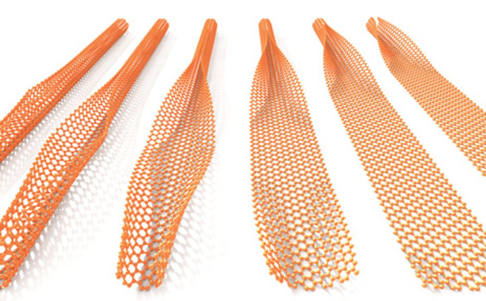
Here’s a better way: Start not with graphite but with a carbon nanotube—essentially a rolled-up sheet of graphene—and unzip it along its length. We do this with a chemical reagent combination known since the 1800s, sulfuric acid and potassium permanganate. Dmitry Kosynkin, a postdoctoral researcher and one of our associates at Rice University, in Houston, discovered the process while trying to oxidize the nanotubes. We found it so remarkable that we spent months accumulating enough evidence to convince ourselves that it worked. The beauty of it is that the chemical reaction can easily be turned into a large-scale process, with a yield approaching 100 percent.
Because carbon nanotubes come in single-walled and many-walled varieties, with diameters from 1 to 100 nm, this process can produce graphene nanoribbons from 3 to 300 nm in width. By selecting the ribbons of the proper size, we can get the building blocks of the particular devices we wish to construct.
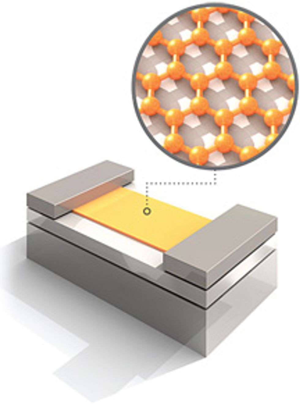
We have taken some of these tube-born ribbons, deposited them on a silicon substrate topped with silicon dioxide, and fabricated them into FETs, which turned out to have electrical properties similar to those of devices that use graphene produced by other techniques. We also demonstrated gating—the inherent property of a FET wherein the transport of carriers is modulated by the third, or gate, electrode—as well as adsorption properties that would make the devices promising for use as sensors and nonvolatile memory.
Although the unzipping process appears promising, there are several problems to solve. First, the graphene nanoribbons are partially damaged by the harsh oxidative environment in the chemical bath, so we are now developing gentler ways to unzip the nanotubes. Second, we need to be able to put the ribbons exactly where we want them, in a way that can be reliably reproduced thousands of times a day in a factory. We’ll also need techniques that can stand the ribbons vertically—like blades of grass—so as to pack more of them into a given area on a chip. Meanwhile, for applications where discrete placement is not required, as in photovoltaic arrays, the graphene ribbons might simply be painted on.
Other techniques to unzip carbon nanotubes are also possible. A group at Stanford has used plasma jets to blow the tops off multiwalled carbon nanotubes while protecting the sides of the tubes under a polymer film. The resulting nanoribbons seem to resist oxidative damage better than the chemically unzipped ribbons do, but it seems there is no way to scale up the fabrication technique. Other researchers have produced graphene using CVD techniques, wafting methane or some other volatile carbon compound onto nickel or copper surfaces, which then catalyze the conversion of those compounds into graphene. It’s also possible to grow graphene epitaxially, by annealing silicon carbide at high temperatures to assemble graphene directly on the SiC wafer, using the carbon atoms that are already there.
This past summer, for instance, researchers at Samsung, together with colleagues from Korea’s Sungkyunkwan University, the National University of Singapore, and Japan’s National Institute of Advanced Industrial Science and Technology, reported using CVD to produce stupendous growth areas, approaching a square meter, on a copper substrate. When the researchers dissolved away the copper, they were able to keep that vast, one-atom-thick sheet of carbon from wrinkling! They also chopped it into transistors, showing the way to mass production. This year IBM achieved another milestone by demonstrating 100-gigahertz graphene-based transistors, and recently a group at the University of California, Los Angeles, set a new record at 300 GHz.
Of course, these transistors are much larger than the silicon variety, but smaller isn’t always better—sometimes faster or more flexible is what you’re looking for. Engineers have already shown that it’s no problem to transfer graphene sheets from a copper growth substrate to a flexible one made of polyethylene terephthalate, the same kind of plastic used in soda bottles. Such devices would be good for transparent, touch-screen displays that roll up when you’re finished using them.
To be sure, silicon will reign supreme in many of the applications in which it is now found. But carbon, silicon’s little brother, has new realms to conquer. And if graphene keeps progressing as fast as it has in the past two years, it will surely attract the immense weight of investment in research and development that has so far gone almost exclusively to silicon. If that happens, then little brother will at first supplement silicon and at last supplant it, as little brothers often do.
About the Authors
Alexander Sinitskii and James M. Tour specialize in the science of the exceedingly small at Rice University, in Houston. Their main interests are the microstructures—nanotubes, sheets, and cages—that carbon atoms tend to form. Tour trained as a synthetic organic chemist, but his work in electronics has led to an extraordinary range of appointments: He’s a professor of chemistry, computer science, mechanical engineering, and materials science, as well as the founder of several companies. Sinitskii, a postdoctoral researcher, earned his doctorate in materials science at Moscow State University.