
Nearly 70 years ago, two physicists at Bell Telephone Laboratories—John Bardeen and Walter Brattain—pressed two thin gold contacts into a slab of germanium and made a third contact on the bottom of the slab. The flow of current through this configuration could be used to turn a small signal into a larger one. The result was the first transistor—the amplifier and switch that was, arguably, the greatest invention of the 20th century. Thanks to Moore’s Law, the transistor has delivered computers far beyond anything thought possible in the 1950s.
Despite germanium’s starring role in the transistor’s early history, it was soon supplanted by silicon. But now, remarkably, the material is poised for a comeback. The world’s leading-edge chipmakers are contemplating a change to the component at the very heart of the transistor—the current-carrying channel. The idea is to replace the silicon there with a material that can move current at greater rates. Building transistors with such channels could help engineers continue to make faster and more energy-efficient circuits, which would mean better computers, smartphones, and countless other gadgets for years to come.
For a long time, the excitement over alternative channels revolved around III-V materials, such as gallium arsenide, which are made from atoms that lie in the columns just to the left and right of silicon in the periodic table of elements. I was active in that research. In fact, eight years ago, I wrote a feature for this magazine heralding the progress that had been made in constructing transistors with III-V channels.
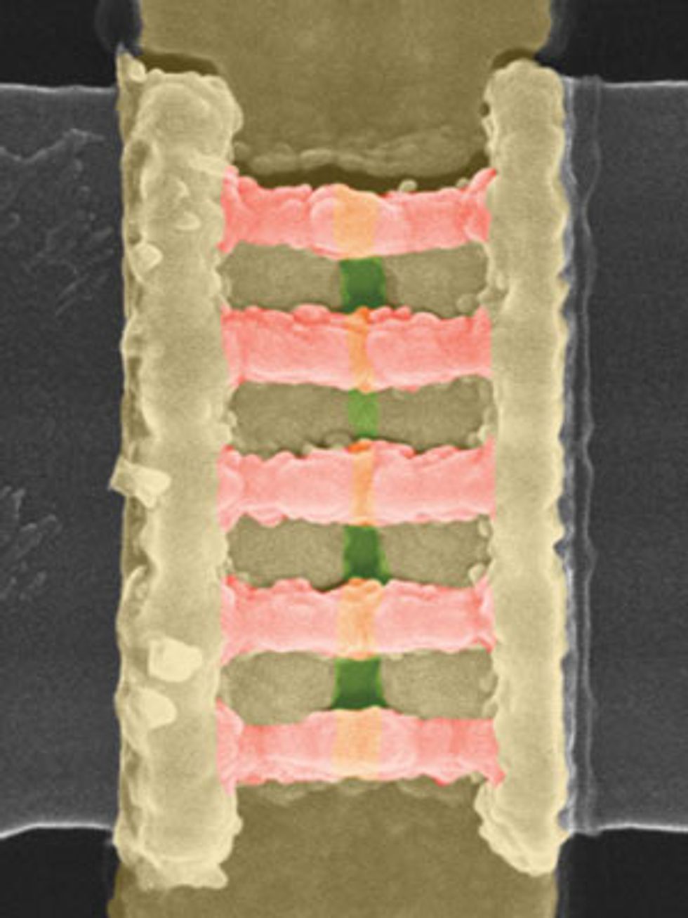
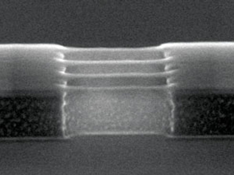 The two transistors in the FinFET-based inverter contain finlike channels, which stand out from the plane of the wafer (top, one set of fins (in pink) from a bird’s-eye view; bottom, an oblique view of another set). The distance between each fin in the top image is in the tens of nanometers.Images: Heng Wu/Purdue University
But as we eventually discovered, the III-V approach has some fundamental physical limitations. It’s also likely to be too expensive and difficult to integrate with existing silicon technology. So a few years ago, my team at Purdue University, in West Lafayette, Ind., began experimenting with a different kind of device: a transistor with a channel made of germanium. Since then, we’ve demonstrated the first complementary-metal-oxide-semiconductor (CMOS) circuits—the kind of logic inside today’s computers—made with germanium grown on ordinary silicon wafers. We have also constructed a range of different transistor architectures using the material. These include nanowire devices, which may be next in line when the present state-of-the-art transistor design, known as the FinFET, can’t be miniaturized any longer.
Best of all, it turns out that putting germanium back into the mix isn’t as big a challenge as it might seem. Transistors that use a combination of silicon and germanium in the channel can reportedly be found in some recent chips, and they made an appearance in a 2015 demonstration of future chip-manufacturing technology by IBM and partners. These developments could be the first steps in an industry trend to adopt the use of higher and higher proportions of germanium in the channel. In a few years’ time, we may find that the material that brought us the transistor has helped usher it into a new age of remarkable performance.
Germanium was first isolated and identified by the German chemist Clemens Winkler in the late 19th century. Named in honor of Winkler’s homeland, the material was long considered a poor conducting metal. That changed during World War II, when germanium’s semiconducting properties—that is, its ability to switch between permitting and blocking the flow of current—were discovered. Solid-state devices based on germanium boomed in the postwar years; U.S. production grew from a few hundred pounds in 1946 to meet a demand for over 45 metric tons of the stuff by 1960. But silicon ultimately won out; it became the material of choice for logic and memory chips.
There are some good reasons why silicon dominated. For one thing, silicon is far more abundant and thus a lot cheaper. Silicon also has a wider bandgap, the energy hurdle that must be overcome in order for a transistor to carry current. The larger the bandgap, the harder it is for current to leak across the device when it’s supposed to be off, draining power. As an added benefit, silicon also has better thermal conductivity, making it easier to draw away heat so that circuits don’t overheat.
Given all those advantages, it’s natural to wonder why we’d ever consider introducing germanium back into the channel. The answer is mobility. Electrons move nearly three times as readily in germanium as they do in silicon when these materials are close to room temperature. And holes—the electron voids in a material that are treated like positive charges—move about four times as easily.
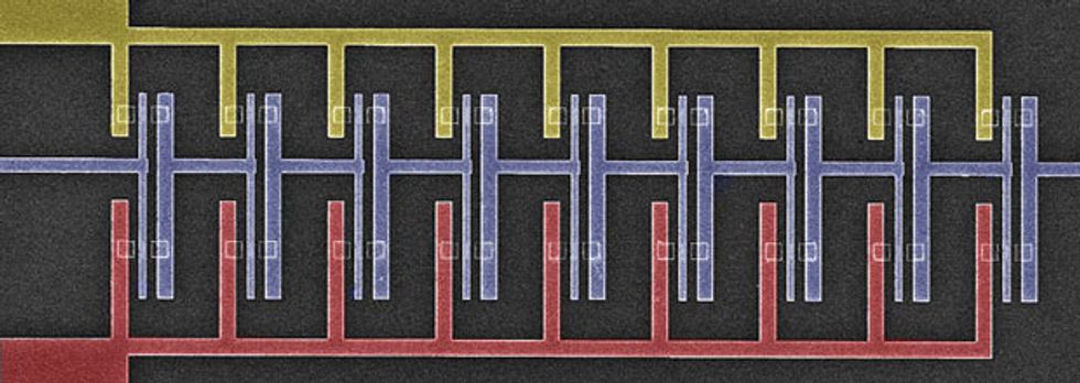 Speedy Circuits: This nine-stage CMOS ring oscillator, presented in 2015, was built on a germanium-on-insulator wafer.Image: Heng Wu/Purdue University
The fact that both electrons and holes are so mobile in germanium makes the material a convenient candidate for constructing CMOS circuits. CMOS employs two different kinds of transistors: the p-channel FET (pFET), whose channel contains an excess of free-moving holes, and the n-channel FET (nFET), which has a similar excess of electrons. The faster these electrons and holes can move, the faster the resulting circuits can be. And because less voltage must be applied to draw those charge carriers along, circuits can also consume considerably less energy.
Of course, germanium isn’t the only such high-mobility material. The III-V compounds mentioned earlier, materials such as indium arsenide and gallium arsenide, also boast excellent electron mobility. In fact, electrons in indium arsenide are nearly 30 times as mobile as they are in silicon. So far, so good. The problem is that this amazing property does not extend to the holes in indium arsenide, which are not much more mobile than holes in silicon. That limitation makes it almost impossible to make a high-performance pFET, and the lack of a fast pFET rules out speedy CMOS circuitry, which is not designed to tolerate a very large difference in the speed between nFETs and pFETs.
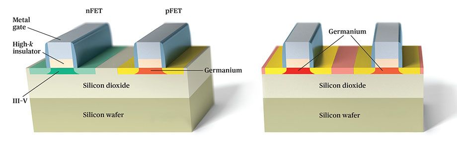
One potential fix is to take the best of each material. Researchers at various institutions, such as the European semiconductor research organization Imec and IBM’s Zurich laboratory, have demonstrated ways to make circuits that build nFET channels from a III-V material and pFET channels from germanium. This technique could lead to very fast circuits, but it also complicates the manufacturing process.
For this and other reasons, we favor a straight-germanium approach. The germanium channels should significantly boost performance, and the manufacturing challenges are expected to be more manageable.
To make germanium—or any alternative channel material—work in mass manufacturing, we must find a way to incorporate the material on the dinner-plate-size silicon wafers that are used to make today’s chips. Fortunately, there are multiple ways to build a germanium layer on a silicon wafer that can then be fashioned into channels. Using a thin layer of the stuff significantly mitigates two key problems with germanium—the fact that the material is costlier than silicon, and that it is a relatively poor conductor of heat.
But replacing silicon in a transistor channel isn’t just a matter of slotting in a thin, high-quality layer of germanium. The channel has to work seamlessly with the other components of the transistor.
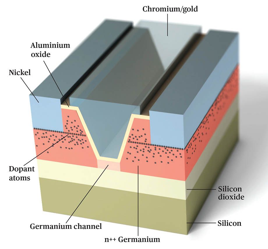
The transistor in today’s ubiquitous CMOS chips is the metal-oxide-semiconductor field-effect transistor, or MOSFET. It has four basic parts. There are the source and drain, which are the origin and destination point for the current; the channel that connects them; and the gate, which is essentially a valve that controls whether current flows through the channel.
In reality, there are several other ingredients inside a state-of-the-art transistor. One of the most critical is the gate insulator, which prevents the gate and channel from short-circuiting. The atoms in semiconductors such as silicon, germanium, and III-V compounds like gallium arsenide are arranged in three dimensions. There is no way to create a perfectly flat surface, so the atoms that sit on the top of the channel will have a few dangling bonds. So what you want is an insulating layer that links up with as many of those dangling bonds as possible, a process called passivation. If it isn’t done well, you’ll wind up with what could be described as an “electrically bumpy” channel, full of places where charge carriers can get temporarily trapped, lowering mobility and therefore the speed of the device.
Happily enough, nature has provided silicon with a high-quality “native” insulator that matches up well with its crystal structure: silicon dioxide (SiO2). Although today’s state-of-the-art transistors contain a more exotic insulator, they still include a thin layer of this native oxide in order to passivate the silicon channel. Because silicon and SiO2 are close structurally, a well-made layer of SiO2 can bind to 99,999 of every 100,000 dangling bonds, which is about how many there are in each square centimeter of silicon.
Gallium arsenide and other III-V materials do not have native oxides, but germanium does, which means it should, in theory, have an ideal material to passivate a germanium transistor channel. The problem is that germanium dioxide (GeO2) is weaker than SiO2, and it can absorb or even be dissolved by the water used to clean wafers during the chip manufacturing process. To make matters worse, it is hard to control the GeO2 growing process. A layer of GeO2 1 or 2 nanometers thick is needed for a state-of-the-art device, but it’s difficult to make layers thinner than about 20 nm.
Researchers have studied some alternatives. Stanford University professor Krishna Saraswat and colleagues, who spurred interest in the idea of using germanium as an alternate channel material way back in the early 2000s, first explored zirconium dioxide, which is a “high-k” insulator of the sort used in today’s high-performance transistors. Building on that team’s work, a group based at Imec, in Leuven, Belgium, examined what could be done with an ultrathin layer of silicon to improve the interface between germanium and such high-k materials.
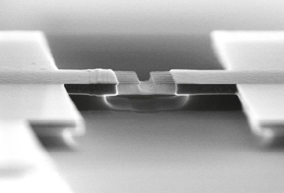
But germanium passivation took a big step forward in 2011, when a team led by Professor Shinichi Takagi of the University of Tokyo demonstrated a way to control the growth of germanium insulator. The researchers first grew a nanometer-thick layer of another high-k insulator, aluminum oxide, on the germanium channel. Once this layer was grown, the ensemble was placed in an oxygen-filled chamber. A fraction of that oxygen passed through the aluminum oxide layer to the underlying germanium, mixing with the germanium to form a thin layer of oxide (a pairing of germanium and oxygen but technically not GeO2). In addition to helping control the growth process, the aluminum oxide acts as a protective cap for this weaker, less stable layer.
 Bridge to Higher Performance: Chipmakers may one day turn to nanowire channels, like these germanium structures. Nanowires can be surrounded by a gate on all sides for added control.Photo: Heng Wu/Purdue University
Several years ago, inspired by this finding, and facing the difficulties involved in creating pFETs with III-V channels, my group at Purdue began investigating ways to build germanium-channel transistors. We began by using germanium-on-insulator wafers, developed by the French wafer manufacturer Soitec. These wafers are standard silicon wafers topped with an electrically insulating layer underneath a 100-nm-thick layer of germanium.
With these wafers, we can build transistors in which all the standard silicon parts—the source, channel, and drain regions—are made of germanium. This is not necessarily the way a chipmaker would opt to make transistors, but it was an easy way for us to start studying the basic properties of germanium devices.
One of the first obstacles we faced was finding a way to handle resistance between the source and drain regions of the transistor and the metal electrodes that connect them to the outside world. This resistance arises from a natural electronic barrier called the Schottky barrier, which forms when a metal and a semiconductor come in contact with one another. Silicon transistors have been endlessly optimized to make this barrier as thin as possible, so that charge carriers have a very easy time tunneling across it. Getting similar behavior in a germanium device, however, requires some smart engineering. Thanks to the nuances of electronic structure, holes move from a metal into germanium quite readily, but electrons don’t. That means nFETs, which rely on the movement of electrons through the device, will have a very high resistance, wasting heat and drawing only a fraction of the current needed for fast circuits.
A standard way of thinning the barrier is to add more dopant atoms to the source and drain regions. The physics are complicated, but think of it this way: More dopant atoms mean more free charges. And with this profusion of free-ranging charge carriers, the electrical interaction between the metal electrodes and the semiconducting source and drain regions is stronger. That stronger coupling tends to promote the tunneling of charges across the barrier.
Unfortunately, this technique does not work as well in germanium as it does in silicon; the material can’t withstand the high concentration of electron-donating dopants that would be needed to thin the Schottky barrier. But what we can do is go where the dopant density is highest.
We can accomplish this by taking advantage of the fact that state-of-the-art semiconductors are doped by using ultrahigh electric fields to push ions into the material. Some of these dopant atoms stop fairly quickly; some go pretty far in. Ultimately, you wind up with a bell-curve-like distribution: The concentration of dopant atoms is highest at some depth and then tapers as you go shallower or deeper. If we recess the source and drain electrodes into the semiconducting material, we can put them in contact with the highest concentration of dopant atoms. That strategy dramatically reduces the contact-resistance problem.
Regardless of whether chipmakers ultimately use this strategy to thin the Schottky barrier in germanium, it is a useful demonstration of what the material is capable of. When we began our research, the best germanium nFETs produced currents of 100 microamperes for each micrometer of width. In 2014, at the Symposia on VLSI Technology and Circuits, in Hawaii, we reported on germanium nFETs with a record drain current of about 10 times that amount and more or less on a par with silicon—not bad for a preliminary demonstration. Some six months later, we reported the first circuits containing both germanium nFETs and pFETs, a prerequisite for making modern logic chips.
Since then, we have used germanium to build more advanced transistor designs, such as FinFETs—the current state of the art. We’ve even made germanium-based nanowire transistors, which could well replace the FinFET in coming years.
These advanced transistor designs will likely be needed for germanium to be adopted in mass manufacturing, because they offer better control over the transistor channel. Thanks to germanium’s small bandgap, a transistor with a germanium channel could require as little as a quarter of the energy that a silicon-channeled transistor needs to switch to a conducting state. This offers the potential for lower-power operation, but it also makes it easier for current to leak through the switch when it’s supposed to be off. A device with better channel control will let chipmakers take advantage of the small bandgap without compromising switching performance.
We’ve made a good start, but we’ve got more work to do. For one thing, there is a need for additional wafer-scale experiments that can demonstrate transistors with high-quality germanium channels. We also need to make refinements to the device design in order to boost the speed.
Of course, germanium is not the only option for tomorrow’s transistor channels. Researchers continue to explore III-V materials, which could be used in addition to germanium or on their own. And there is a dizzying array of other potential improvements to transistors—and the way they are wired together—on the horizon. That list includes carbon-nanotube transistors, vertically oriented switches, 3D circuits, channels made from a mix of germanium and tin, and transistors that operate by a process called quantum tunneling.
We may end up adopting several of these technologies in the coming years. But adding germanium to the channel—even initially mixed in with silicon—is a solution that will allow chipmakers to keep improving transistors in the near term. Germanium, the primordial material of the solid-state age, could be a powerful elixir for its next decade.
This article appears in the December 2016 print issue as “Switching Channels.”
About the Author
Peide D. Ye is a professor of electrical and computer engineering at Purdue University in Indiana.