
In July 1962, the Telstar 1 satellite took an enormous leap toward the globally connected world we now take for granted. It relayed from space, for the first time ever, live television images and telephone calls between continents: specifically, a ground station in Andover, Maine, and other stations in England and France. It accomplished this feat thanks to a microwave repeater that had at its heart a slight but powerful vacuum device known as a traveling-wave tube. The 30-centimeter-long, glass-walled electron tube was at the time the only device capable of boosting a broadband television signal with enough power to cross an ocean. Solid-state devices just weren’t up to the task.
More than a half century later, traveling-wave-tube amplifiers still dominate satellite communication. That’s right—your ultrahigh-definition satellite TV and satellite radio come to you courtesy of vacuum tubes in space.
Of course, there’s a huge difference between Telstar’s 3.5-watt, 4-gigahertz amplifier and one of the dozens of highly efficient microwave amplifiers on, say, the DirecTV-15 satellite, launched earlier this year. The latest generation of traveling-wave tubes can provide up to 180 W at frequencies up to 22 GHz, with efficiencies approaching 70 percent and rated lifetimes exceeding 15 years. Though their basic function is the same—amplifying RF signals—just about everything else has changed: the design, the testing, the materials, and the fabrication.
That’s my point. In the six decades since vacuum tubes lost out to solid-state devices in computers, receivers, and power supplies, vacuum technology has continued to evolve and branch out into new terrain, sustaining a small but skilled corps of engineers and scientists around the world, as well as a multibillion-dollar industry. That’s because the traveling-wave tube and other vacuum devices continue to serve one purpose extremely well: as powerful sources of microwave, millimeter-wave, and submillimeter-wave radiation. (Vacuum tubes are also used in amplifiers for musical instruments and high-end audio, but the tubes I’m talking about are for generating radio-frequency waves, not audio waves.) What’s more, they do it efficiently and over broad bandwidths, and compactly and reliably, too. And by virtue of their construction and the metals and ceramics from which they’re fashioned, traveling-wave tubes are inherently hardened against radiation (unlike solid-state devices) and fairly impervious to temperature and mechanical extremes. Besides satellite communication, traveling-wave tubes are widely used in radar, electronic warfare, and other military systems.
And now, ongoing research into a new and potentially revolutionary kind of traveling-wave tube—the ultracompact and ultraefficient cold-cathode TWT—looks poised to deliver the first practical device by the end of this decade. These are exciting times for vacuum tubes. Here’s why.
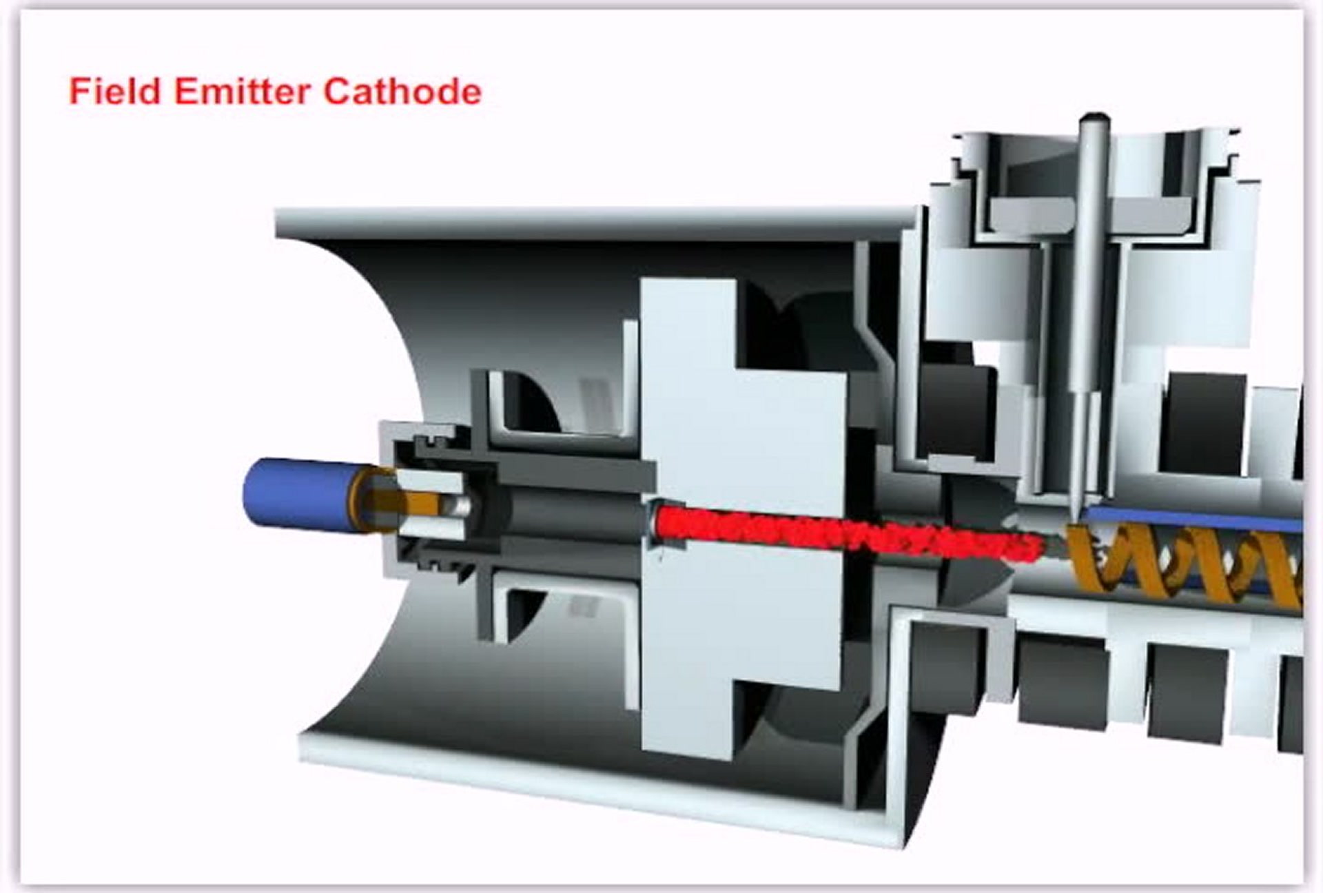
The Traveling-Wave Tube: Then and Now

For amplifying radio-frequency signals, nothing beats a traveling-wave tube. Here, we see a modern TWT [top] and one from the 1950s [bottom]. In both cases, the cathode is heated to emit an electron beam, which is injected into a helix-shaped circuit.
The RF signal to be amplified is injected onto the helix, with the resulting electromagnetic wave extending away from the helix and exerting a force on the incoming beam. Unmodulated as it entered the helix, the beam current now has an RF component. The modulation induces electromagnetic fields on the helix, which then act on the electrons, and the RF signal grows exponentially.
In a modern traveling-wave tube, the beam power that is not converted to RF is recovered by the depressed collector, which acts like the regenerative brakes on a hybrid car and boosts the overall efficiency to 65 percent or more. That feature plus other advances in design, testing, materials, and fabrication have allowed TWTs to continue to outperform solid-state RF sources. And recent research on a cold-cathode TWT promises to revolutionize vacuum electronics. —C.M.A.
“If the transistor had been invented first, the vacuum tube would have been invented immediately afterwards.” That remark, by vacuum electronics great Robert S. Symons, was his standard comeback against frequent attacks that his was an antiquated field of legacy devices soon to be eclipsed by semiconductors. Those of us who followed in Symons’s footsteps of course agree that the tube’s compelling attributes make it worthy of pursuit, but unfortunately we still contend with that same prejudice against the technology.
Not that we have a, er, chip on our shoulder, but in what ways are tubes superior? Let’s review. At its heart, an RF source, whether solid-state or vacuum electronics, is a power converter, changing some fraction of the incoming electricity into RF power. The input power is a product of the incoming current times the incoming voltage. Traveling-wave tubes operate at high voltage—typically from a few kilovolts to tens of kilovolts—which means they need only a little current to produce a very powerful electron beam. True, you need a fabulous power supply to feed the tube, but advances in compact high-voltage electronics have solved that problem.
Solid-state devices used in RF sources, by contrast, operate at low voltage—typically 8 to 10 volts for sources based on gallium arsenide and up to about 70 V for gallium nitride sources. So to get a high output power, the current also needs to be high, which can then create excessive heat that stresses the chip’s connections. The upshot is that to equal the output of, say, a single 300-W traveling-wave tube, you’ll need to gang a bunch of solid-state devices together, which adds to the complexity and cost of your design; even then, the efficiency of your RF source will be at best only about half that of a modern TWT.
To appreciate how a tube does what it does, let’s consider its basic parts: an electron gun (consisting of a cathode that’s heated to generate a beam of electrons, an anode to accelerate the beam to high velocity, and in most cases a beam-controlling gate electrode near the cathode to switch the cathode current on and off); an electromagnetic circuit that interacts with the electron beam; a collector for capturing the electron beam as it exits the interaction circuit; and a focusing magnet, for confining the electron beam as it propagates through the tube. The first three parts—the electron gun, interaction circuit, and collector—reside in a hard vacuum (about 10-8 pascals), while the magnet sits outside the vacuum. We create the vacuum by heating the tube to over 500 °C for more than 24 hours, which cleans the inner surfaces of the tube and drives out residual gas. The walls of a modern tube are made not of glass but of heat- and corrosion-resistant metals like tungsten and molybdenum, as well as iron, high-purity copper, and high-temperature ceramics.
So here’s how the traveling-wave tube works: First, the electron gun injects an electron beam through the center of the interaction circuit; the most common type of circuit used in traveling-wave tubes is shaped in a helix. The RF signal to be amplified is then injected onto the helix. The resulting electromagnetic wave extends away from the helix and so exerts a force on the incoming beam of electrons. The first electrons entering the helix will accelerate in the direction of the beam; a half cycle later, the entering electrons will slow down. As the beam travels through the circuit, the faster electrons will overtake the slower ones so that bunches of electrons form.
The result is that the beam current, which was unmodulated as it entered the helix, now has an RF component at the signal frequency. The modulation in turn induces electromagnetic fields on the helix, which then act on the electrons; as a result, the signal on the helix grows exponentially—that is, we get gain. But because power must be conserved, this increase in the RF signal’s strength comes at the expense of the beam’s kinetic energy, and so the beam slows down.
 Inner Tube: An x-ray of a traveling-wave tube from
TMD Technologies, a UK manufacturer of vacuum devices. Shown here is the tube's collector, which recovers some of the energy from the electron beam, thereby boosting the device's efficiency.Photo: TMD Technologies
Inner Tube: An x-ray of a traveling-wave tube from
TMD Technologies, a UK manufacturer of vacuum devices. Shown here is the tube's collector, which recovers some of the energy from the electron beam, thereby boosting the device's efficiency.Photo: TMD Technologies
Even so, on its pass through the circuit, only about a quarter to a third of the beam power is typically converted to RF, which means the beam exiting the circuit still retains a lot of power. To recover some of that kinetic energy, we slow the beam down further using something called a depressed collector, which is basically a series of electrodes that operate like the regenerative brakes on a hybrid car. A modern space-based traveling-wave tube has a depressed collector with four or five stages, which can recover well over 80 percent of the exiting beam energy, resulting in overall efficiencies of 65 percent or more. The tube also has fins attached to the collector to radiate heat from the tube and the satellite into the cold surroundings of space. A solid-state device has no analogue to the depressed collector.
Because of the tube’s exquisitely low vacuum and the beam’s near-perfect focus, very little energy is lost due to collisions as the beam passes through the circuit. The electrons in solid-state devices, by contrast, suffer a multitude of collisions as they drift through the semiconductor, and so produce waste heat right at the transistor junction, inside the device itself. It’s not hard to see why heat removal is one of the biggest challenges for high-power solid-state devices. And in contrast to TWTs, their performance is much more sensitive to variations in operating temperature.
So what’s responsible for the major leaps in performance and efficiency from the Telstar era to today? In a way, solid-state and vacuum devices have followed parallel paths over the past 50 years, benefiting from advances in computational design, engineered materials, and microfabrication.
Computer modeling and simulation, for instance, allow engineers to model a tube from the cathode to the collector and everything in-between, with the result that it’s commonplace to have prototypes work on the first pass, something unthinkable just 10 years ago. And tube designers can now create previously unimaginable multiple-beam vacuum devices, like Northrop Grumman Corp.’s multiple-beam traveling-wave tube, which provides an astounding 50 W of pulsed power at 214 GHz. The tube uses five separate electron beams rather than a single beam, so it can operate at lower voltage and requires less magnetic focusing. Understanding the complex three-dimensional physics involved in producing, focusing, and capturing those beams and modeling their conversion to RF power could be done only using modern computational tools.
Meanwhile, advances in microfabrication are making it possible to actually build these new designs. Researchers at the University of California, Davis, have used high-speed micromachining—with tool bits barely visible to the naked eye and spinning at rates exceeding 50,000 revolutions per minute—to create metallic structures with dimensional accuracies in the micrometers. Such fine structures are what you need to produce the extremely high frequencies typical of today’s most sophisticated traveling-wave tubes. Borrowing a page from the semiconductor industry, engineers at Northrop Grumman and Teledyne Scientific Co. have etched traveling-wave-tube circuits onto silicon wafers. And in an extension of a MEMS technique, researchers at the U.S. Naval Research Laboratory are using a process that combines UV lithography and electroplating to make extremely accurate, all-metal structures for use in millimeter-wave traveling-wave tubes. Given the pace of advances in additive manufacturing, 3-D–printed components for vacuum tubes can’t be that far off.
Engineered materials, too, are fomenting a minor revolution in vacuum-device manufacture. I’m guessing you’ve never heard of nanocrystalline scandium oxide–doped tungsten powder, but it is behind the biggest advance in tube cathodes in decades.
As mentioned, the cathode is the source, or emitter, of the electron beam that flows through a tube. Most tubes use thermionic emitters, which emit a copious stream of electrons when heated to around 1,000 °C. (You can sear a steak at 400 °C.) The most common type of cathode consists of a barium mixture dispersed within a porous tungsten matrix. Heated, the barium continuously diffuses to the surface, forming a thin oxide layer. This layer is said to have a “work function,” which is just a measure (expressed in electron volts) of how difficult it is to extract an electron from it. The lower the work function, the lower the temperature you need to emit electrons, the lower the evaporation rate of the barium, and the longer the cathode lasts. The cathode life basically triples for every 0.2 electron volt’s reduction in the work function. Today’s cathodes have work functions of about 2.0 eV; applying a thin metal coating lowers the work function to 1.8 eV.
Now, the cathode’s operating temperature is determined by its current density—that is, the amount of current emitted per unit area. Careful control of the current density in space-based traveling-wave tubes means the cathodes can last up to 20 years; terrestrial tubes, which typically operate at higher current densities, have shorter lives, of about seven years. But tube designers are always on the lookout for materials that will reduce the work function and thereby extend the tube’s life.
Thus the interest in scandium oxide. Researchers have known for years that scandate cathodes, made from tungsten and scandium oxide, have low work functions. But attempts to turn them into practical, commercial components always fell short. Recently, however, Yiman Wang and her colleagues at the Beijing University of Technology demonstrated that cathodes made from nanocrystalline powders of scandium oxide and tungsten resulted in a robust emitter with a work function of 1.43 eV, more than tripling the life of a standard traveling-wave-tube cathode. This advance also allows you to operate such a cathode at a higher current density, which would vastly simplify the focusing of the fine electron beams needed in higher-frequency millimeter- and submillimeter-wave tubes.
As great as the scandate cathode sounds, imagine if you replaced the thermionic emitter with a cathode that didn’t need to be heated at all. That would be truly revolutionary. Vacuum engineers even have a name for such a device: the cold-cathode traveling-wave tube. A cathode that operates at ambient temperature would have all sorts of advantages: You wouldn’t need a heater; the cathode wouldn’t wear out; there’d be no warm-up time for the tube—it would essentially be instant on and off; and the current density could be much higher because its emission wouldn’t be limited by the operating temperature. What’s more, you could modulate the beam’s current right at the cathode, as is done in the high-power tubes used for UHF TV transmitters, only now it would be at microwave frequencies. Cold-cathode vacuum devices would usher in a new generation of ultracompact, high-fidelity, high-efficiency amplifiers, which could be used, for instance, in powerful yet tiny RF transmitters on small satellites.
This video explains how a cold-cathode traveling-wave tube operates compared to a traditional TWT:
No surprise, then, that researchers have sought the cold-cathode traveling-wave tube for decades. Charles “Capp” Spindt and Kenneth Shoulders of SRI International, in Menlo Park, Calif., were among the first to articulate its virtues, in a 1966 paper entitled “Research in Micron-size Field Emission Tubes.”
While there are various ways of emitting a beam of electrons without heating, the one that Spindt and Shoulders described nearly 50 years ago is still the most promising: field emission. All you need to make it work is a strong electric field at the surface between the emitter and the vacuum. Ordinarily, free electrons in a metal at room temperature encounter an energy barrier near the metal’s surface that keeps them confined. But when you heat the metal—as in a thermionic emitter—you’re giving some of those electrons enough energy to overcome the barrier.
Instead, let’s apply an inward-directed electric field at the surface, which exerts an outward force on the electrons and thins the barrier; as the field increases, the barrier is thinned still more. To achieve high field emission at the level you would need in a traveling-wave tube, the barrier must be so thin that the electrons leak right through it. In quantum mechanical terms, the electrons have “tunneled” through the barrier. To get significant numbers of electrons to escape, you’ll need to apply a very high electric field, of more than a billion volts per meter. For comparison, during a thunderstorm a local electric field of around 2,000 volts per meter is considered dangerous.

 Cones in Wells: The cold-cathode traveling-wave tube developed by researchers at SRI International and L-3 Electron Devices relies on up to 50,000 micrometer-size molybdenum cones, each of which can emit a tiny beam of electrons at room temperature. The tube itself is shown in the opening photo of this article.Photos: SRI International (2)
So how do you get a high field without having to apply excessively high voltage? The answer lies in nanofabrication. We know that the electric field between two conducting electrodes gets stronger as the electrodes are brought closer together. So if we bring the positively charged gate electrode (that is, the electrode that modulates the emission from the cathode) and the negatively charged emitter very close together—as in less than a micrometer apart—a strong inward electric field results at the surface of the emitter. We also shrink the emitter features to the nanometer scale and take advantage of the field enhancement that occurs naturally at sharp edges and points, sort of like a nano lightning rod. Now you have a field-emitter cathode that operates at less than 100 V.
To date, the best-performing cold-cathode device, as measured by total emission current and current density, was demonstrated by Spindt, Christopher Holland, and Paul Schwoebel at SRI. Their cathode consists of tens of thousands of micrometer-size molybdenum cones deposited on a circular silicon substrate with an area of about one square millimeter. Each cone acts as an electron emitter and sits in its own well, carved into a 2.5-micrometer-thick silicon-dioxide insulating layer. A thin metal coating over the insulating layer serves as the gate electrode for the array of field emitters.
For more than a decade, my colleague David Whaley and I, working with the SRI team, have been trying to turn this laboratory device into something more practical. Milestones to date include the first operation of a 100-W cold-cathode TWT at a frequency of 4 to 6 GHz and the first 100-milliampere electron beam generated by a cold cathode. Whaley and I also demonstrated a TWT with current densities from the cold cathode exceeding 15 amperes per square centimeter, which far exceeds the typical 2 A/cm2 from a thermionic cathode. The current density from our cathode was so high, in fact, that to get the beam to travel through the helix, we had to expand the beam first rather than compress it.
The cathode worked well for more than 150 hours before breaking down electrically. Breakdown is a major challenge for these field emitters because of the high fields within the structure and the thin-film gate electrode. An electrical short between the gate and any one of the thousands of emitter cones will burn out the entire array of emitters and render it unusable.
Recently, our colleagues at SRI have developed a feature to mitigate the damaging effects of such shorts. They interrupt the electrical breakdown path between the base of the cones and the gate by adding a dielectric layer between them—a shield, if you will. My company, L-3 Electron Devices, tested one of these SRI cathodes in a traveling-wave tube that generated up to 10 W at 18 GHz—a record-high frequency for a cold-cathode device. Testing showed that the cathode was much more resistant to, and tolerant of, individual emitter failures.
One challenge we’re still addressing is the traveling-wave tube’s high operating voltage. While the field-emitter cathode can emit electrons at around 100 V, you need a much higher voltage to accelerate and focus the electron beam coming from the cathode to interact with the helix circuit. But you also need to avoid any high-voltage arcs between, for example, the anode and the field-emitter cathode. We’re also working on ways to prevent stray ions from traveling back upstream and striking the cathode’s gate and field emitter tips. In our TWT, we’ve created an electrostatic ion barrier to prevent such ions from making it to the cathode.
While much work remains on the cold-cathode TWT, I’m confident we will have a practical device within five years. Advances like this one underscore the ongoing relevance and vitality of vacuum electronics, even after more than a century of development. Maybe that’s why the Defense Advanced Research Projects Agency announced in August a pair of new programs aimed at pushing the field even further. Vacuum technology continues to smash through performance barriers and open up new areas of application. It refuses to fade into obscurity.
NOTE: The views are those of the author.
About the Author
Carter M. Armstrong, an IEEE Fellow, is vice president of engineering at the Electron Devices Division of L-3 Communications, in San Carlos, Calif. His September 2012IEEE Spectrumarticle “The Truth About Terahertz” dissected the hype surrounding T-ray devices.