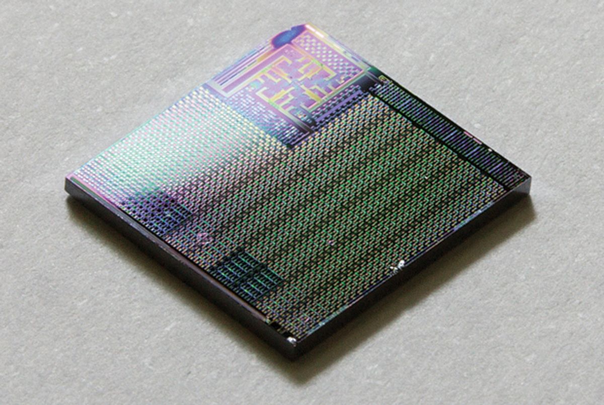
Working with the Korea Advanced Institute of Science and Technology (KAIST), NASA is pioneering the development of tiny spacecraft, each made from a single silicon chip, that could slash interstellar exploration times.
Speaking at the IEEE International Electron Devices Meeting in San Francisco last December, NASA’s Dong-Il Moon detailed this new technology, which is aimed at ensuring such spacecraft survive the potentially powerful radiation they’ll encounter on their journey.
Calculations suggest that if silicon chips were used to form the heart of a spacecraft powered by a tiny, featherweight solar sail and accelerated by a gigawatt-scale laser system, the craft could accelerate to one-fifth the speed of light. At such high speeds, it would reach the nearest stars in just 20 years, compared with the tens of thousands of years it would take a conventional spacecraft.
Moon and coworkers argue that 20 years in space is still too long for an ordinary silicon chip, because on its journey it will be bombarded by more high-energy radiation than chips encounter on Earth. “You are above most of the magnetic fields that block a lot of radiation, and above most of the atmosphere, which also does a good job of blocking radiation,” says Brett Streetman, who leads efforts in chip-scale spacecraft at the Charles Stark Draper Laboratory, in Cambridge, Mass.
Radiation leads to the accumulation of positively charged defects in the chip’s silicon dioxide layer, where they degrade device performance. The most serious of the impairments is an increase in the current that leaks through a transistor when it is supposed to be turned off, according to Yang-Kyu Choi, leader of the team at KAIST, where the work was done.
Two options for addressing chip damage are to select a path through space that minimizes radiation exposure and to add shielding. But the former leads to longer missions and constrains exploration, and the latter adds weight and nullifies the advantage of using a miniaturized craft. A far better approach, argues Moon, is to let the devices suffer damage but to design them so that they can heal themselves with heat.
“On-chip healing has been around for many, many years,” says Jin-Woo Han, a member of the NASA team. The critical addition made now, Han says, is the most comprehensive analysis of radiation damage so far.
This study uses KAIST’s experimental “gate-all-around” nanowire transistor. These devices use nanoscale wires as the transistor channel instead of today’s fin-shaped channels. The gate-all-around device may not be well known today, but production is expected to rocket in the early 2020s. [See “Transistors Could Stop Shrinking in 2021,” IEEE Spectrum, August 2016.]
The gate—the electrode that turns the flow of charge through the channel on or off—completely surrounds the nanowire. Adding an extra contact to the gate allows you to pass current through it. That current heats the gate and the channel it surrounds, fixing any radiation-induced defects.
Nanowire transistors are ideal for space, according to KAIST, because they naturally have a relatively high degree of immunity to cosmic rays and because they are small, with dimensions in the tens of nanometers. “The typical size for [transistor dimensions on] chips devoted to spacecraft applications is about 500 nanometers,” says Choi. “If you can replace 500-nm feature sizes with 20-nm feature sizes, the chip size and weight can be reduced.” Costs fall too.
KAIST’s design has been used to form three key building blocks for a single-chip spacecraft: a microprocessor, DRAM memory for supporting this, and flash memory that can serve as a hard drive.
Repairs to radiation-induced damage can be made many times, with experiments showing that flash memory can be recovered up to around 10,000 times and DRAM returned to its pristine state 1012 times. With logic devices, an even higher figure is expected. These results indicate that a lengthy interstellar space mission could take place, with the chip powered down every few years, heated internally to recover its performance, and then brought back to life.
Philip Lubin, a professor at the University of California, Santa Barbara, believes that this annealing-based approach is “creative and clever” but wonders how much danger from cosmic rays there really will be to these chips. He would like to see a thorough evaluation of existing technologies for chip-scale spacecraft, pointing out that there are already radiation hardened electronics developed in the military.
Today, efforts at NASA and KAIST are focusing on the elimination of the second gate contact for heating. This contact is not ideal because it modifies chip design and demands the creation of a new transistor library, which escalates production costs. Those at KAIST are investigating the capability of a different design, called a junctionless nanowire transistor, which heats the channel during normal operation. Separately, at NASA, researchers are developing on-chip embedded microheaters that are compatible with standard circuits.
Cutting the costs of self-healing tech will play a key role in determining its future in chip-scale spacecraft, which will require many more years of investment before they can get off the ground.


