Just weeks after we were presented with the prospect of three-color infrared imaging, researchers at the University of Sydney in Australia have potentially turned the field of infrared technology on its ear with a new approach that could make infrared technology extremely inexpensive to produce.
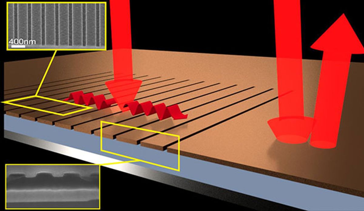
In research described in the journal Optica, the Australian scientists have demonstrated you don’t need exotic materials like metamaterials to achieve total light absorption, which means zero light is either reflected or transmitted. Instead they turned to conventional materials that are compatible with optoelectronic applications such as photodetectors and optical modulators and etched 41-nanometer-thick antimony sulfide grating structures on them.
Total light absorption (TLA) is key for devices such as infrared night-vision goggles and has been both a holy grail and a challenge to achieve. The belief has been that if devices can be fabricated that are capable of TLA, then they could be useful in a variety of things beyond night-vision goggles, including photodetectors, optical switches, modulators, and transducers.
While other research groups have fabricated devices that approach this TLA, they depended on difficult-to-produce nanostructures or on expensive special materials. The Australian researchers believe their approach is simpler and can be used with a fairly wide range of light absorbing materials.
“By etching thin grooves in the film, the light is directed sideways and almost all of it is absorbed, despite the small amount of material – the absorbing layer is less than 1/2000th the thickness of a human hair,” said Martijn de Sterke, who led the research, in a press release.
The structure consists of a 130nm thick silver reflector as a substrate. A silicon dioxide layer 245nm thick is layered on top of that and used a spacer. At this point the 41nm-thick layer of amorphous antimony sulfide is deposited by thermal evaporation. Then the grating is fabricated by using electron-beam lithography to define the mask in an acrylic glass resist, with the etching being performed by a plasma gas.
The key to the low cost of this approach is that the total light absorption can be achieved with just about any naturally occurring weak absorbers.
As the paper explains:
“Ultrathin perfect absorbers made of weakly absorbing semiconductors may be used in optoelectronic applications such as photodetectors, where the use of semiconductors provides the possibility of extracting a photocurrent or measuring the photoresistivity.”
With high-quality infrared detectors costing around $100,000 and some of the materials used requiring low-temperature cooling, a simple and inexpensive approach could prove a boon for the technology.
“There are many applications that could greatly benefit from perfectly absorbing ultra-thin films, ranging from defence and autonomous farming robots to medical tools and consumer electronics,” said Björn Sturmberg, co-lead author of the research, in the press release.
Dexter Johnson is a contributing editor at IEEE Spectrum, with a focus on nanotechnology.


