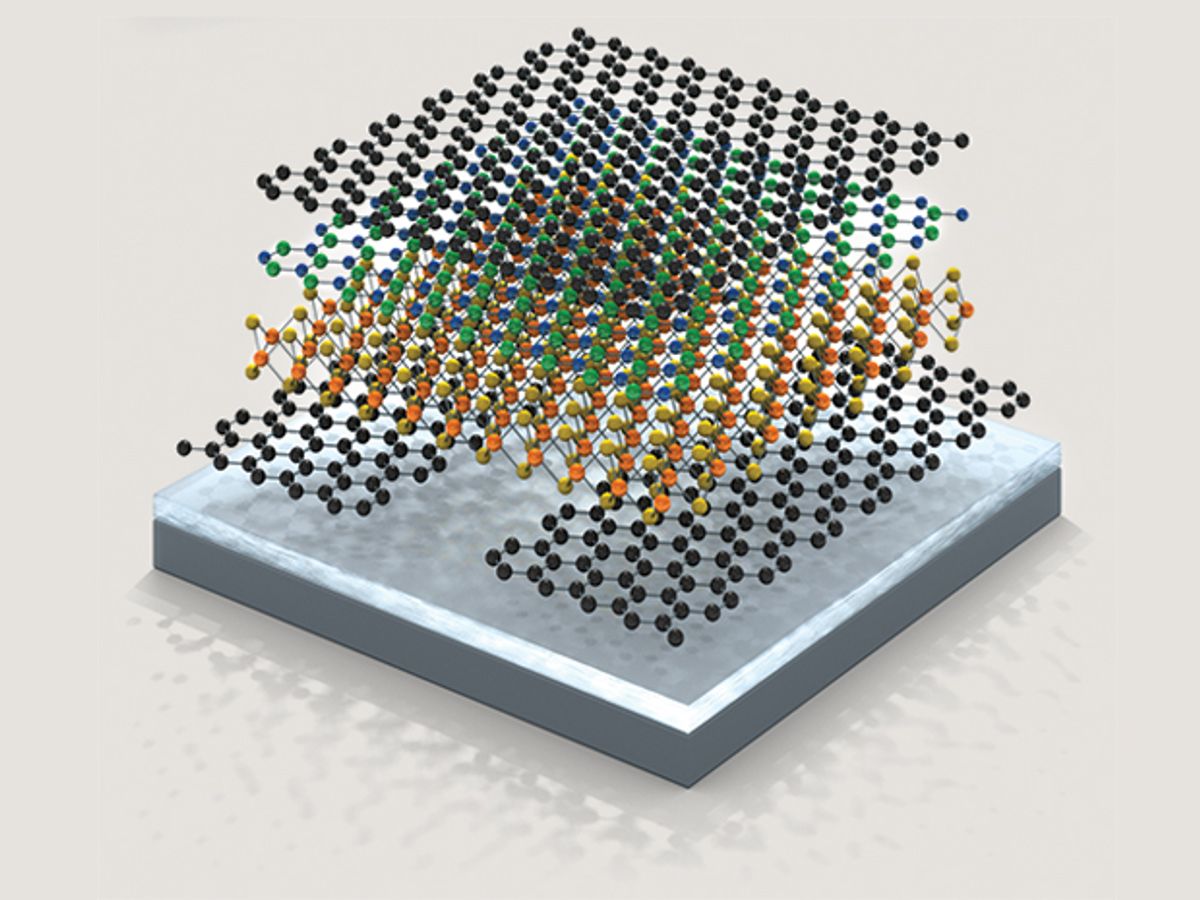
Last April, two separate research projects reported building transistors made entirely from two-dimensional (2-D) materials. Researchers at Argonne National Laboratory described in the journal Nano Letters that they had produced a transparent thin-film transistor (TFT) made from tungsten diselenide (WSe2) as the semiconducting layer, graphene for the electrodes and hexagonal boron nitride as the insulator.
Then, one week later, the journal ACS Nano published work from researchers at Lawrence Berkeley National Laboratory who had also built an all 2-D transistor that took the shape of a field emission transistor (FET). The Berkeley Lab FET had the same materials for its electrode and insulator layers as Argonne's TFT, but used molybdenum disulfide (MoS2) as the semiconducting layer.
While the fabrication of transparent TFTs made entirely from 2-D materials could lead to flexible displays with a super-high density of pixels, the impact of an all-2-D FET could have a broader impact. That's because FETs are nearly ubiquitous, used in computers, mobile devices and just about every other electronic system you can think of.
With that in mind, the Berkeley Lab researchers are beginning to put their achievement of an all-2-D FET into perspective, describing in more detail some of the possibilities of their 2-D FET technology.
One of the problems that has plagued FETs prior to their work has been that their charge-carrier mobility degrades because of mismatches between the crystal structure and the atomic lattices of the individual components, namely the gate, source and drain electrodes. These mismatches result in rough surfaces and in some cases dangling chemical bonds. The all-2-D FET developed at Berkeley Lab eliminates this issue by creating an electronic device in which the interfaces are based on van der Waals interactions, which represent all the attractive or repulsive forces between molecules that are not covalent bonds, instead of covalent bonding.
"In constructing our 2D FETs so that each component is made from layered materials with van der Waals interfaces, we provide a unique device structure in which the thickness of each component is well-defined without any surface roughness, not even at the atomic level," said Ali Javey, a faculty scientist in Berkeley Lab's Materials Sciences Division, in a press release.
He added that the approach "represents an important stepping stone towards the realization of a new class of electronic devices." By relying on interfaces based on van der Waals interactions rather than covalent bonding, it will be possible to achieve an "unprecedented degree of control in material engineering and device exploration."
"The results demonstrate the promise of using an all-layered material system for future electronic applications," he said.
Dexter Johnson is a contributing editor at IEEE Spectrum, with a focus on nanotechnology.


