It’s heady times in power electronics. After decades of domination by silicon, two newer materials—silicon carbide and gallium nitride—have begun taking over multibillion-dollar markets. Silicon carbide is now the semiconductor of choice for the inverters and chargers in electric vehicles, for example. And if you’ve purchased a wall charger lately for your smartphone or laptop, chances are good that it uses gallium nitride.
The newer materials, known as wide-bandgap semiconductors, are taking over these and other power-electronics applications because they offer many superior characteristics. And yet wide-bandgap technologies still have fundamental weaknesses. For a silicon-carbide transistor, a big one is relatively low mobility of electrons in the channel—the area under the device’s gate through which current flows between the source and the drain. That low mobility prevents SiC transistors from switching at high rates. That, in turn, limits their efficiency in applications such as converting between alternating current and direct current. Gallium-nitride transistors, on the other hand, have a quirk known as “dynamic on-resistance,” which means that when the device is conducting current, the resistance of the device depends on the voltage—higher voltage means higher on-resistance. Another problem with GaN is that the physical size of the device, and therefore its cost, goes up as its voltage-blocking capability does, a significant flaw for devices expected to turn on and off voltages that are many times higher than those found inside, say, a typical computer.
What if you could combine GaN and SiC in a single device that minimizes the weaknesses of each and maximizes their strengths? That’s the question that drove a team of 16 researchers at the Hong Kong University of Science and Technology and three other institutions in China. After years of work, they finally claimed success by fabricating a transistor, which they call a hybrid field-effect transistor, or HyFET. They described their work in a paper presented at the IEEE International Electron Devices Meeting, held this past December in San Francisco.
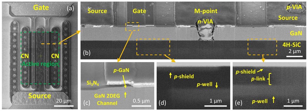 A scanning-electron microscope (SEM) image of a HyFET, looking down at the device [a], clearly shows the gate and a source. A cross-sectional SEM image of the HyFET [b] shows the gallium nitride transistor at the top and the silicon carbide below. Other SEM images show the gate region of the GaN device [c], and the channel of the SiC transistor [d and e]. The Hong Kong University of Science and Technology
Experts in wide-bandgap semiconductors not involved with the research were impressed with the technical achievement. “I actually am very excited about the results of Kevin Chen’s group in Hong Kong,” said IEEE Fellow Debdeep Jena, a professor and laboratory leader at Cornell University. “It has a lot of merit and promise.” However, these experts’ opinions about the device’s commercial prospects were generally more circumspect.
In operation, the device uses a low-voltage, high-speed GaN transistor to control a high-voltage SiC junction field-effect transistor (JFET). In a conventional SiC JFET, the drain is at the bottom of the device, connected to the substrate. Current flows vertically, controlled by a gate on top of the device, through a “drift layer” to one or more source terminals, also on top of the device. In the HyFET, that basic configuration is recognizable: There’s a drain at the bottom of the device, connected to the substrate. Current flows upward through a SiC drift layer. However, the gate and source terminals are in a GaN transistor integrated directly above the SiC JFET, at the top of the device. So the current flowing through the SiC JFET is controlled by a gate and source terminals that are in the GaN part of the device.
The advantage here is that it is the GaN transistor, with its high electron mobility, that controls the switching of the combined device. And built on the foundation of the SiC JFET, with its large drift region, the combined device has the voltage-blocking capabilities of SiC. Testing indicated that the device largely fulfilled the researchers’ expectations. Although the mobility is not quite as high as for a conventional GaN device, it is “suitable for high-frequency switching,” they found. They also demonstrated that in the “off” state, the device could block around 600 volts, depending on temperature—not bad for a first-of-its-kind experimental device.
Many challenges had to be surmounted to fabricate the device. One of the major ones was growing a GaN transistor directly on top of an SiC one. Gallium nitride devices are routinely fabricated on substrates of SiC. However, these devices are grown “on axis,” meaning they are grown layer by layer with each layer parallel to the substrate. But SiC devices are typically grown off axis with respect to the orientation of their substrate crystal’s lattice. So the researchers had to devise a means of growing a GaN transistor on top of an SiC device with a deviance from the axis, or “miscut,” of 4 degrees.
To do this they developed a technique that they call two-step biaxial strain release. A fundamental problem with the interfaces between two different semiconductors is the strain created at the boundary where the two dissimilar crystals merge. This strain can create performance-robbing imperfections in the lattice called dislocations. The technique refined and exploited by the researchers releases the strain through two specific kinds of dislocations, minimizing its detrimental effects.
One of the weaknesses of the HyFET is its resistance to current flow when the transistor is in the on state. This value, called specific on-resistance (specific Ron), is quite high, at around 50 milliohms - cm2. Higher Ron means lower overall efficiency. Of course, the HyFET is literally the first of its kind, built in a university laboratory.
“The large Ron in our paper results from a small device...and a very conservative design in the SiC portion,” wrote author and IEEE Fellow Kevin Chen in an e-mail. “In general, there are no additional obstacles toward the realization of 3 mΩ∙cm2 (~2.6) for a 1,200-V HyFET with industrial SiC manufacturing facilities.”
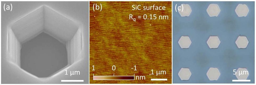 Scanning electron images show a hole, or via, in the gallium nitride portion of the device [a]. When filled with metal [c], these vias become conductive pathways, enabling current to flow between the gallium-nitride and silicon-carbide portions of the device. An image made with atomic force microscopy [b] shows the surface of a silicon-carbide layer.The Hong Kong University of Science and Technology
For comparison, though, a state-of-the art SiC or GaN transistor capable of blocking more than 600 volts can have Ron as low as 2 mΩ∙cm2, notes IEEE Life Fellow B. Jayant Baliga, the inventor of the insulated-gate bipolar transistor and Distinguished University Professor of Electrical Engineering at North Carolina State University. Given these figures, Baliga questions how much demand there would be for a commercial HyFET, when much simpler and probably cheaper SiC transistors are available. “What would motivate someone to shift to something much more complicated, with all these layers being grown, if the specific on-resistance is not reduced below that of the silicon-carbide MOSFET [metal oxide semiconductor FET]?” Baliga asked.
IEEE Fellow Umesh Mishra, Dean of the College of Engineering at the University of California Santa Barbara, and a pioneer in GaN power devices, questioned whether the advantages of integrating two different semiconductors into a single device—minuscule inductive delays and capacitive losses—were worth the costs in manufacturing complexity and other factors. To manufacture such a device, a company “now has to have two technologies that they’re running in the fab,” he notes. “They have to have silicon-carbide technology, and they have to have gallium-nitride technology. Nobody wants to do that because you now have two complicated technologies that you are simultaneously trying to run”—a costly proposition.
“To scale something difficult is always hard,” Mishra adds. “Then the question is, what is your benefit?” Mishra notes that most of the advantages of the combined device could be obtained at much lower cost by simply connecting the two different transistors together in a single package, rather than integrating them into a single hybrid device.
Author Chen, however, suggested that unwanted electronic characteristics, particularly a weakness called parasitic inductance, would plague transistors that are simply packaged together rather than integrated. “Lower parasitic inductance minimizes switching oscillation and reduces switching loss,” he wrote in his e-mail. “Advanced co-packaging techniques could reduce the parasitic inductance to a certain degree, but may not be as cost effective as the integrated device (realized in a batch process).”
Jena, at Cornell, noted that a potentially insurmountable obstacle for the HyFET is the rate of advancement of GaN devices, in particular. In the foreseeable future, he says, GaN will become so capable that it probably won’t require hybrid schemes to triumph. “The physics tells me that GaN is the winner in the long run,” he says. “I don’t want to take anything away from the [HyFET] paper. It’s a great paper. But whatever they have shown here will also be possible with gallium nitride in the future,” he concludes.