
We cherish our smartphones for delivering entertainment and information on the go, but their need for daily charging is a problem. Battery life can’t get any shorter than it is today. (Well, it could, but consumers wouldn’t be happy about it.) So when new smartphone models come on the market with microprocessors based on the latest foundry process, the increase in the number of transistors in the chips should be balanced by a reduction in the power that each transistor consumes.
For the remainder of the decade, this power reduction per transistor can be accomplished with today’s workhorse device: the silicon FinFET. (It’s so named because the channel through which current flows is shaped like a vertical fin.) But continuing progress further into the future will require an overhaul of the transistor’s architecture: If the devices unveiled in December at the IEEE International Electron Devices Meeting (IEDM) are an indication, that overhaul will see the FinFET’s silicon fin shrink vertically to become a nanometers-wide wire made from semiconductors other than silicon.
The superior semiconducting alternatives include germanium and III-V materials (so called because they combine a group III element such as gallium with a group V element such as arsenic). They transport charge faster and allow the production of transistors that can deliver the same amount of current as their silicon counterparts but at a lower voltage, saving power.
The change in geometry from fin to wire saves power in a different way: The gate, whose voltage controls the flow of current through the channel, can surround four sides of a nanowire channel but only three sides of a fin. So in the nanowire configuration, the gate is more effective at pinching off unwanted current that might otherwise leak through the channel, again saving power.
The building blocks of the CMOS circuits of today’s processors require two types of transistors: one that transports electrons and another that carries holes, their positive counterparts. At IEDM, Peide Ye, a professor of electrical and computer engineering at Purdue University, in West Lafayette, Ind., championed germanium-based nanowire transistors for both types of devices. Meanwhile, a team of researchers from universities in Singapore showcased the promise of an all–III-V approach, and Niamh Waldron, principal engineer at Imec, the European microelectronics center, reported performance advances yielded by the pairing of an electron-transporting III-V transistor with a hole-transporting germanium transistor.
All three approaches have their pros and cons. Ye, who has spent a great deal of time over the past 15 years improving the performance of III-V transistors, argues that germanium devices are much easier to process. But the National University of Singapore’s Xiao Gong points out that there are difficulties associated with making electron-transporting germanium transistors. Among the challenges: forming good electrical contacts.
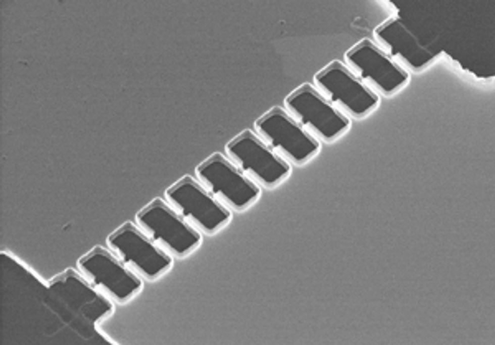 Odd Wire Out: Eleven nanowires form the channel to balance the germanium transistor’s performance.Image: Purdue University
Aaron Thean, vice president of logic at Imec, touts the European center’s approach, which pairs a germanium hole-transporting transistor with a III-V electron-carrying device. He says it is best from a pure performance standpoint.
Fundamentally, the problem they all have to solve is how to marry their materials to the silicon that makes up the rest of the transistor and the chip substrate. That’s a challenge because of the significant difference in the atomic spacing of crystalline silicon and that of germanium and III-V films. Consequently, depositing these materials onto silicon tends to lead to defects that destroy device performance.
But researchers think they’ve got the problem licked. “I think we have finally bridged that gap,” says Waldron.
For Imec, the process for making these nanowire devices draws heavily on its in-house technology for making III-V–based FinFETs. Here, the III-V crystals are grown in V-shaped grooves in silicon, and the majority of the defects you’d ordinarily get are annihilated when the growing crystals meet the groove walls. To change a fin into a nanowire, one part of the fin, composed of indium phosphide, is etched away to leave indium gallium arsenide (InGaAs) nanowires.
Waldron and her colleagues first reported encouraging initial results for their InGaAs nanowires in 2014. They have now improved them by introducing a new process, developed in conjunction with ASM International, for adding an undisclosed material to the gate.
Electrical measurements at an operating voltage of 0.5 volt—which is about two-thirds of that used in circuits made with Intel’s most modern process—highlight the superiority of the new gate. Transconductance, which reflects how quickly charge carriers move in the channel, has almost doubled to 2,200 microsiemens per micrometer.
The other key characteristic for assessing the suitability of these transistors is the subthreshold swing. This is related to the switching capability of the device and is governed by the quality of the interface between the transistor’s channel and its gate dielectric.
For Imec’s devices, the subthreshold swing is 110 millivolts per decade. (In other words, it takes 110 mV at the transistor gate to increase the current tenfold.) “We have to get it down for it to be a true contender” for next-generation CMOS, admits Waldron, who believes progress can be made by reducing the density of defects in the III-V layers. Still, she says, “I think this is a very big step forward for the technology. We are really confident for the future.”
Ye’s team has realized the far lower value of 64 mV per decade. “It’s as good as you can wish,” says Ye, who explains that FETs have a fundamental limit of 60 mV per decade.
This excellent result for subthreshold swing is the culmination of several years of hard work, which began with the development of a process for forming a good contact on electron-transporting germanium FETs and then doing so with germanium FinFETs. “Now we have moved even further,” says Ye. “At this year’s IEDM, we [presented] the first nanowire-based germanium CMOS.”
The nanowire devices also yielded a transconductance of 1,057 μS/µm, which is a record for electron-transporting germanium nanowire FETs. These devices were combined with their hole-transporting cousins to form an inverter circuit with a gain approaching that of a silicon nanowire inverter. Although Ye’s inverter operated at 1 V, he believes this could be trimmed to 0.5 V by further improving the contacts.
An advantage of an all-germanium approach is that it avoids many complications of crystal growth. Ye’s team simply purchased a wafer from the French firm Soitec that had a silicon base bonded to the combination of an insulating oxide and a layer of germanium. Making the nanowires was then just a case of etching material away.
Like Ye and his colleagues, the Singapore team began with a germanium-on-insulator wafer. But they then had to grow several gallium-based semiconductors on it to produce nanowires of indium arsenide and gallium antimonide. In order to bridge the large difference in the atomic spacing between a gallium arsenide layer grown on the wafer and that of the gallium antimonide and indium arsenide layers, they developed a growth process that ensures that every 14th gallium atom at the interface does not bond with antimony.
“At around 10 nanometers from the interface, the quality of the material is very good, so we can grow the...channel layers,” says Gong, of the Singapore team. The total thickness for the layers bridging the difference in lattice spacing is just 150 nm, compared with roughly 1 μm for traditional buffer layers, meaning less material, lower costs, and faster production.
The first devices created by the Singapore team produce low currents and high subthreshold swing, but they expect improvements to come along with the use of higher-quality material and a more suitable etching process for the gate.
There is much work to do before any of these technologies are ready for device production in the 2020s. Imec seems to be closest. But “there is work to be done,” says Thean.
This article originally appeared in print as “Rise of the Nanowire Transistor.”


