
Light-based quantum technology could enable virtually unhackable communication networks and computers that can tackle problems that are currently unsolvable. Today, generating exotic quantum states of light requires bulky equipment that limits the scalability of any potential applications. A new device that squeezes all the necessary components onto a chip smaller than a coin could be the solution, say researchers.
Most of the headline-grabbing results in quantum computing have come from processors that use superconducting qubits, but companies like Xanadu and PsiQuantum are betting that encoding quantum data in photons could be a more powerful approach. Photons are also the obvious choice for quantum communication networks, because they are compatible with existing fiber-optic technology and their quantum states are relatively stable.
A critical capability for both applications is the ability to generate pairs of photons that are entangled, where the quantum states of the two particles are intrinsically linked no matter how large the distance between them. This makes it possible to link many qubits in a quantum processor to generate exponential speedups on certain problems. It’s also the key to connecting the nodes of a quantum-communication network in ways that are impervious to attempts at eavesdropping.
Advances in photonics have made it possible to entangle photon pairs on a chip rather than using bulky optical equipment, which could greatly expand the scope of the technology. But the photons themselves still have to be generated by a conventional laser, says Michael Kues, a professor at the Leibniz University of Hannover in Germany. “You have everything on this small chip, but you still have this big laser,” he says. “That makes it kind of bulky and also not really mass-producible, and that limits scalability.”
In a new paper published 17 April in Nature Photonics, Kues and his colleagues unveil the first photonic chip that integrates all of the key components required to generate entangled photon pairs. Their approach relies on merging two different kinds of semiconductor technology to create a hybrid chip that can both generate laser light and convert that light into high-quality entangled photons. “This is now all in one tiny device smaller than a one euro coin,” says Kues.
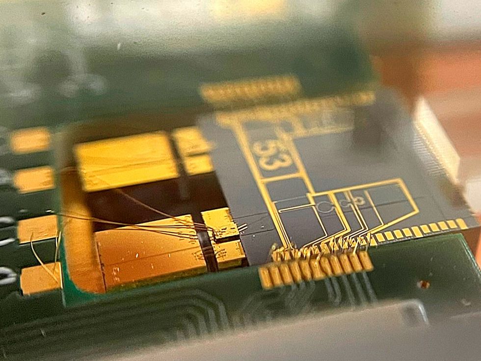 The size of the light source is reduced by a factor of more than 1,000 by using a novel “hybrid technology” that combines a laser made of indium phosphide and a filter made of silicon nitride on a single chip.Institute of Photonics/LUH
The first section of the chip features an optical amplifier built out of indium phosphide, a material that has already been widely used to create semiconductor lasers. This material isn’t suitable for generating entangled photons though, so the researchers connected that section of the chip via a waveguide to a second section made from silicon nitride. This features a series of “microring resonators”—circular waveguides that the laser light is forced to shuttle around—that get progressively smaller.
The first two rings are designed to filter out noise from the laser signal, which can interfere with the quantum states the researchers are trying to create. As the light circulates around the final ring, two laser photons of different frequencies are annihilated to generate a pair of entangled photons. The chip draws about 3 watts of power and is able to produce 8,200 pairs of entangled photons per second at optical communications wavelengths (1,550 nanometers is the most common wavelength used for fiber optics).
“All the parts of this work have been demonstrated before; however, the integration of all of them together is an achievement,” says Amr Helmy, a professor of photonics at the University of Toronto. In particular, he says that incorporating an innovative filtering mechanism on the same chip as the other components is a significant accomplishment. However, it appears to come at the expense of performance, says Helmy, with the brightness of the output and quality of the quantum states falling short of prior work.
Nonetheless, the researchers say that the ability to shrink the size of a quantum light source by a factor of 1,000 could help to bring the technology out of the lab and make it easier to deploy in the real world. As well as more obvious uses in quantum computing and quantum networking, Kues says the compact form factor could also prove useful for some quantum sensing applications.
However, despite the fact that both the semiconductor technologies the team relied on are already in use in industry, the process of integrating the two could be a potential barrier to mass production. At present the two sections of the chip have to be aligned manually to ensure the waveguides match up, which would be a difficult process to scale up, says Kues. “We’ve demonstrated now that the functionality is possible, but to really build it there’s still a lot of research to do,” he adds.
- Quantum Entanglement Meets Superconductivity in Novel Experiment ›
- What Is Quantum Entanglement? ›
- Faster, More Secure Photonic Chip Boosts AI Training - IEEE Spectrum ›


