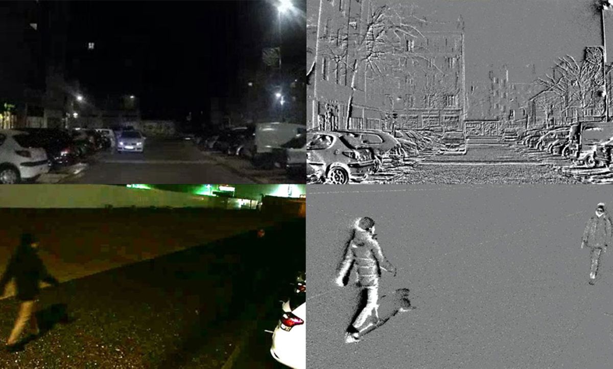
There’s something inherently inefficient about the way video captures motion today. Cameras capture frame after frame at regular intervals, but most of the pixels in those frames don’t change from one to the other, and whatever is moving in those frames is only captured episodically.
Event-based cameras work differently; their pixels only react if they detect a change in the amount of light falling on them. They capture motion better than any other camera, while generating only a small amount of data and burning little power.
Paris-based startup Prophesee has been developing and selling event-based vision sensors since 2016, but the applications for their chips were limited to systems that needed only VGA resolution. The sensor resolution was limited because the circuitry surrounding the light-sensing elements took up so much space. In a partnership announced this week at the IEEE International Solid-State Circuits Conference in San Francisco, Prophesee worked with Sony to put that circuitry on a separate chip that sits behind the pixels.
“Using the Sony process, which is probably the most advanced process, we managed to shrink the pixel pitch down to 4.86 micrometers” from their previous 15 micrometers, says Luca Verre, the company’s cofounder and CEO.
Conventional versus stacked pixel designIllustration: Prophesee
The resulting 1280 x 720 HD event-based imager is suitable for a much wider range of applications, including surveillance and monitoring, augmented reality, virtual reality, and drones.
The company is also looking to enter the automotive market, where imagers need a high dynamic range to deal with the big differences between day and night driving. “This is where our technology excels,” he says.
Besides the photodiode, each pixel requires circuits to convert the diode’s current into a logarithmic voltage and determine if there’s been an increase or decrease in luminosity. It’s that circuitry that, in the new sensors, is put on a separate chip that sits behind the pixels and is linked to them by a dense array of copper connections. Previously, the light-sensing area made up only 25 percent of the area of the pixel, now it’s 77 percent.
When a pixel detects a change (an event), all that is output is the coordinates of the pixel, the polarity of the change, and a 1-microsecond-resolution time stamp. The imager consumes 32 milliwatts to register 100,000 events per second and ramps up to just 73 milliwatts at 300 million events per second. A system that dynamically compresses the event data allows the chip to sustain a rate of more than 1 billion events per second.
This post was corrected on 21 February to clarify the Sony partnership and the applications for the new sensor.
Samuel K. Moore is the senior editor at IEEE Spectrum in charge of semiconductors coverage. An IEEE member, he has a bachelor's degree in biomedical engineering from Brown University and a master's degree in journalism from New York University.


