
Semiconductor lasers, unlike bulky gas lasers and fiber lasers, are tiny, energy efficient, and highly controllable. The one thing they can’t do is deliver their competitor’s steel-slicing brightness.
In results reported last week in Nature, a group of researchers at Kyoto University, in Japan, led by IEEE Fellow Susumu Noda, has taken a big step in overcoming the limitations of semiconductor laser brightness by changing the structure of photonic-crystal surface-emitting lasers (PCSELs). A photonic crystal is composed of a semiconductor sheet punched through with regular, nanometer-scale air-filled holes. Photonic crystal lasers are attractive candidates for high-brightness lasers, but until now engineers haven’t been able to scale them up to deliver beams bright enough for practical metal cutting and processing.
(Brightness is a figure of merit that encompasses a laser’s output power and beam quality and encapsulates how well a beam of light can be focused or how little it diverges. The threshold for metal work is about 1 gigawatt per square centimeter per steradian.)
Slicing Stainless Steel With a PCSELyoutu.be
Noda’s group, which has been working on PCSELs for more than two decades, was able to develop a laser with a diameter of 3 millimeters, a tenfold areal jump up from previous 1-millimeter-diameter PCSEL devices. The new laser has a power output of 50 watts, a similar increase from the 5- to 10-W power output of the 1-mm PCSELs. The new laser’s brightness, about 1 GW/cm2/str, is now high enough for applications currently dominated by bulky gas lasers and fiber lasers, such as precision smart manufacturing in the electronics and automotive industries. It’s also high enough for more exotic applications such as satellite communications and propulsion.
Increasing the photonic crystal lasers’ size and brightness did not come without challenges. Specifically, semiconductor lasers encounter problems when their emission area is expanded. A larger lasing area means there is room for light to oscillate in the direction of emission as well as laterally.
These lateral oscillations, called higher-order modes, can ruin the beam’s quality. Furthermore, if the laser is operating continuously, heat inside the laser changes the device’s refractive index, causing the beam’s quality to deteriorate even further. Noda’s group used photonic crystals embedded within the laser, combined with adjustments to an internal reflector, to allow single-mode oscillation over a wider area and to compensate for thermal disruption. These two changes allowed the PCSEL to maintain high beam quality even while continuously operating.
In a typical photonic crystal laser, the holes—which have a different refractive index from the surrounding semiconductor—cause light within the laser to deflect in a precise way. Noda’s group designed the pattern of holes in the crystal so that light is deflected by an array of circular and elliptical holes staggered one-quarter of the laser light’s wavelength apart. Those deflections cause losses in the higher-order modes, resulting in a high-quality beam that barely diverges.
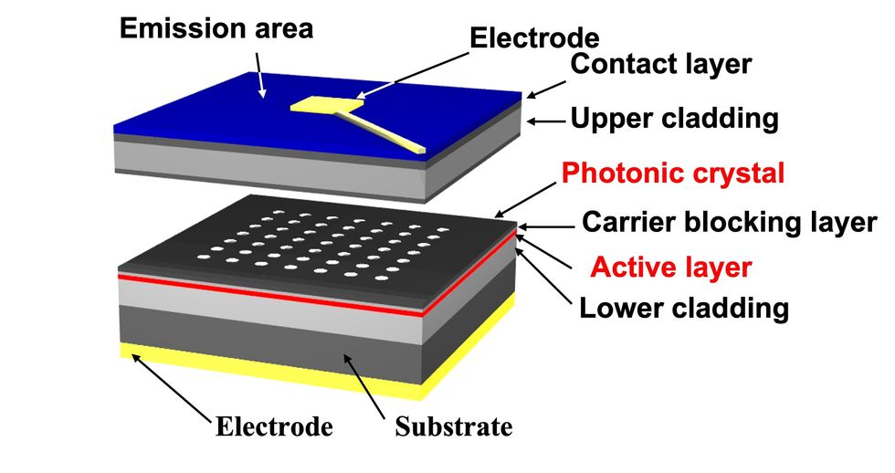 Photonic-crystal surface-emitting lasers (PCSELs) emit light from the top. The photonic crystal boosts brightness.Susumu Noda
That concept worked well enough for the 1-mm laser, but scaling it up to 3 mm required further ingenuity. To allow single-mode operation over a large area, the position of the laser’s bottom reflector was adjusted to cause more loss of unwanted modes in the vertical direction. Finally, Noda’s group dealt with the problem of heat altering the device’s refractive index and causing the beam to diverge. The solution to that problem was to slightly modify the period of the air holes in the photonic crystal, so that they were in the right position to do their job when the laser was at full power.
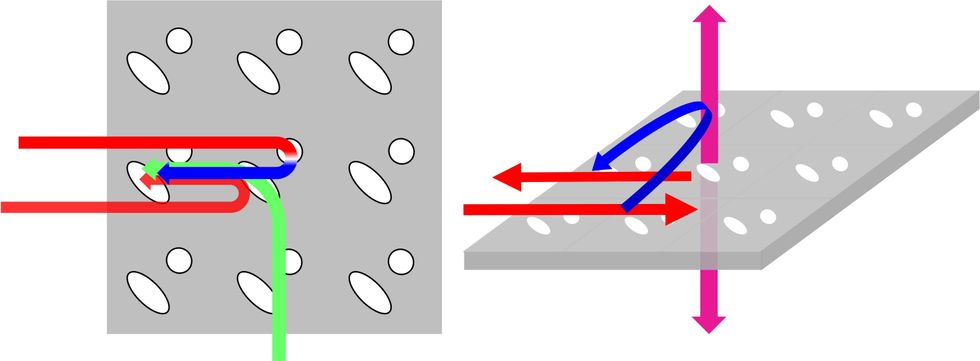 The shape and pitch of air holes in a photonic crystal cause unwanted laser modes to refract and interfere with each other [left]. For the 3-millimeter laser [right] an additional source of unwanted modes had to be dealt with using the laser’s bottom mirror [not shown].Susumu Noda
Noda and his group established the 1,000-square-meter Center of Excellence for Photonic-Crystal Surface-Emiting Lasers at Kyoto University, where more than 85 companies and institutes are involved in developing PCSEL technology. The team is in the process of industrializing their PCSEL design for mass manufacture.
As part of that process, they have made the switch from manufacturing the photonic crystal with electron-beam lithography to making it with nano-imprint lithography. Electron-beam lithography is precise, but usually too slow for mass manufacturing. Nano-imprint lithography, which basically stamps a pattern into a semiconductor, is useful in creating very regular patterns quickly.
Noda explains that the next steps are to continue scaling up the diameter of the laser from 3 to 10 mm, a size that could produce 1 kilowatt of output power—although the goal could also be reached using an array of 3-mm PCSELs. He expects that the same technology that led to the 3-mm devices could be used to scale up to 10 mm. “The same design is enough,” Noda says.
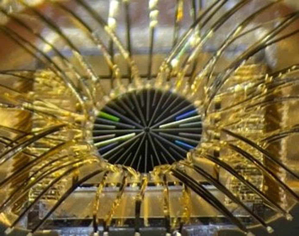 It takes 110 amperes to bring the laser to full power, which necessitates many electrodes.Susuma Noda
- Supremely Small BICSEL Laser Traps Light in Open Air ›
- Experiment Reveals the Peculiar Way Light Travels in a Photonic Crystal ›
- The Top 10 Semiconductor Stories of 2023 - IEEE Spectrum ›


