Empirical evidence is continuing to pile up confirming that so-called topological insulators—materials that behave as conductors near their surfaces but act as insulators throughout the bulk of their interiors—do exist.
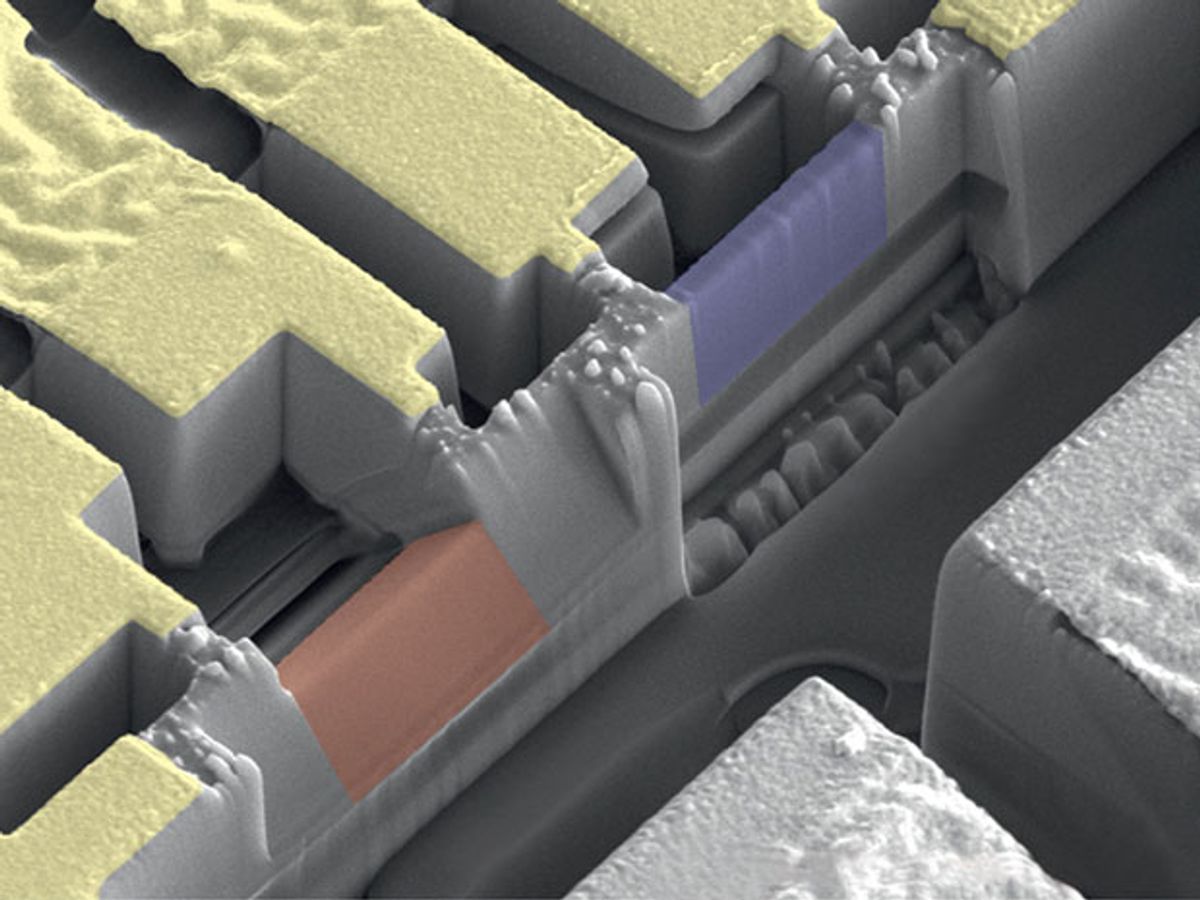
Now, researchers at the Department of Energy’s Lawrence Berkeley National Laboratory (Berkeley Lab), in cooperation with the Max Planck Institute for Chemical Physics of Solids, in Germany, have produced a new type of topological matter. It can carry an electrical current on its surface at room temperature and then get that electrical current to transport itself to the other side of the material. The key to performing this trick was producing nanoscale slices of a material called cadmium arsenide, an inorganic semimetal that is a semiconductor.
What is intriguing about cadmium arsenide is that it exhibits some of the same electronic properties as graphene. Researchers from Oxford, Stanford, and the University of California, Berkeley discovered in 2014 that electrons within cadmium arsenide act as though they have no mass at all, just as they do in graphene. But unlike graphene, cadmium arsenide is a stable 3D material that is comparatively easy to produce in bulk and simple to fabricate for use in electronic devices.
In research described in the journal Nature, the team used focused-ion beams to shape the cadmium arsenide so that electrons rotated around one side of the material as if they were on a racetrack and then traveled through the bulk of the material to rotate on the other side. One of the implications for this kind of movement is the ability to transport charge and energy through a material without loss.
“This had been theorized by Andrew Potter [an assistant physics professor at the University of Texas at Austin] on our team and his coworkers, and our experiment marks the first time it was observed,” said James Analytis, a staff scientist at Berkeley Lab and assistant professor of physics at UC Berkeley, in a press release. Analytis, who led the research, added that “it is very unusual—there is no analogous phenomena in any other system. The two surfaces of the material ‘talk’ to each other over large distances due to their chiral nature.”
Chirality is a quantum property in which a particle’s (in this case an electron’s) spin is coupled to its momentum, providing it with clear left-handed or right-handed properties. In this experiment, the researchers observed that the motion of the electrons possessed a dual handedness. In other words, some electrons traveled around the material in one direction while others moved in the opposite direction. The researchers believe that this experiment shows a way toward exploiting this chirality to transport charge and energy through a material without loss. Researchers have predicted that this would alleviate much of the overheating experienced in today’s chips as dimensions become ever smaller.
In the experiments, the researchers applied an electric current to slices of cadmium arsenide only 150 nanometers thick; electrons began to race around in circles until their path took them through both the surface and the bulk of the material.
When the researchers applied a magnetic field to the material, it pushed the electrons around the surface. When the surface electrons reached the same energy and momentum of the bulk electrons, they were pulled by the chirality of the bulk and pushed through to the other surface. This strange back-and-forth motion is repeated until defects in the material completely scatter the electrons.
The scientists say that, in future research, they would like to use fabrication techniques on the cadmium arsenide that build the magnetic properties directly into the material so that an external magnet will not be required to achieve this effect.
If they’re successful, then it’s possible to foresee its use in fabricating interconnects between computer chips in so-called spintronic devices, which exploit the spin of an electron rather than its electrical charge to process data.
Dexter Johnson is a contributing editor at IEEE Spectrum, with a focus on nanotechnology.


