Last year we saw confirmation that 3-D printing had emerged into the mainstream. Six years ago, companies like MakerBot were the only ones showing their 3-D wares at CES. Last year, the Consumer Electronics Association dedicated an entire show floor at CES to 3-D printing, only to have it sell out and then sell out again after space was added.
While 3-D printing has been exploding, 3-D imaging of objects so they can be translated into 3-D-printed products has been lagging behind—keeping it an expensive option and outside the reach of most amateur 3-D printing enthusiasts.
Now researchers at CalTech have changed that by developing an inexpensive 3-D imaging device that can be integrated into a smartphone. The imager, they say, can send data to a 3-D printer that will allow it to reproduce a copy accurate to within micrometers of the original object’s dimensions.
The device the CalTech team developed is called a nanophotonic coherent imager (NCI); it employs an inexpensive silicon chip to produce the highest depth-measurement accuracy of any nanophotonic 3-D imaging device ever created.
An ordinary digital camera logs information about the intensity of light at a certain point in the image, it doesn’t capture any data regarding the distance of the light at that point. The NCI is able to provide information both on the intensity of light as well as its relative distance.
“Each pixel on the chip is an independent interferometer—an instrument that uses the interference of light waves to make precise measurements—which detects the phase and frequency of the signal in addition to the intensity,” said Ali Hajimiri, a professor at CalTech, in a press release.
In the research, which was published in the journal Optics Express, the team employed LIDAR, which is a laser imaging system, to illuminate the target object with scanning laser beams. When the light bounces off the target object, it is analyzed based on the wavelength of laser light that was used. Through this analytical process it becomes possible to determine the object’s size and distance from the laser and thereby create a 3-D image of the object.
“By having an array of tiny LIDARs on our coherent imager, we can simultaneously image different parts of an object or a scene without the need for any mechanical movements within the imager,” Hajimiri said in the release.
The optical technique being exploited here is called coherence, where two light waves share the same frequency and therefore the same peaks and troughs. When the imager illuminates an object with this coherent light, the light is reflected back and is picked up by grating couplers that serve as pixels, or image sensors. The imager basically uses the coherent light as a standard to measure against the reflected light that comes off the objects.
One of the key developments of this technology was the small size they were able to achieve for the device.
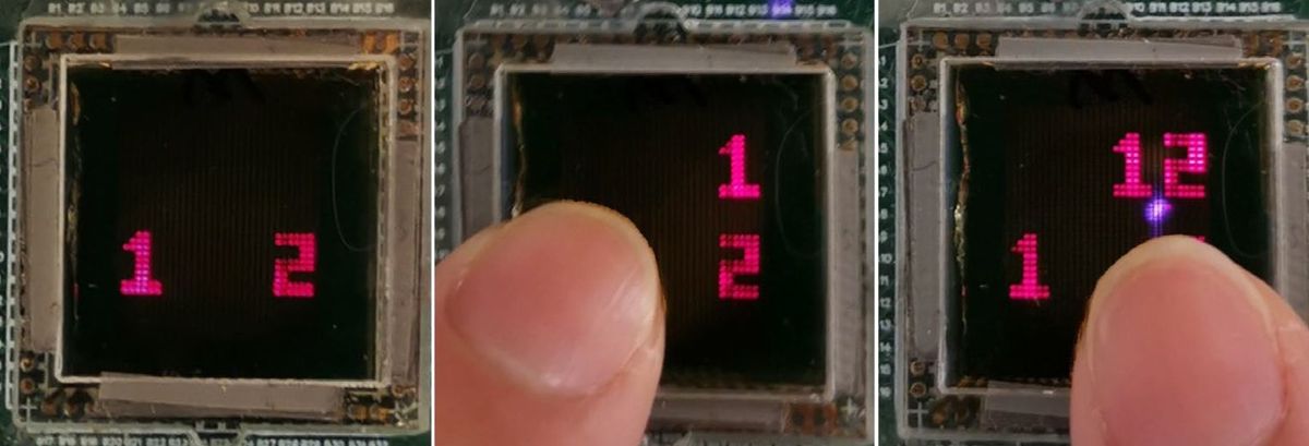
“By coupling, confining, and processing the reflected light in small pipes on a silicon chip, we were able to scale each LIDAR element down to just a couple of hundred microns in size—small enough that we can form an array of 16 of these coherent detectors on an active area of 300 microns by 300 microns,” Hajimiri said.
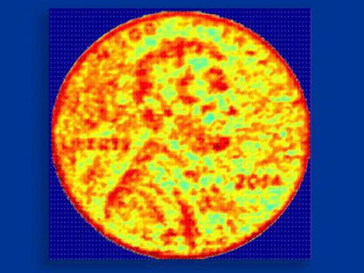
While the first proof-of-concept device only had 16 pixels, the researchers were able to overcome this limitation by imaging four-pixel-by-four-pixel sections and then moving the object by four pixel increments. Using this method, the researchers were able to image the face of a U.S. penny.
The researchers are confident that in future iterations of the device they can scale up to hundreds of thousands of pixels. In this case, the device could be used for more than 3-D imaging; it could find applications in collision prevention in driverless cars.
Dexter Johnson is a contributing editor at IEEE Spectrum, with a focus on nanotechnology.


