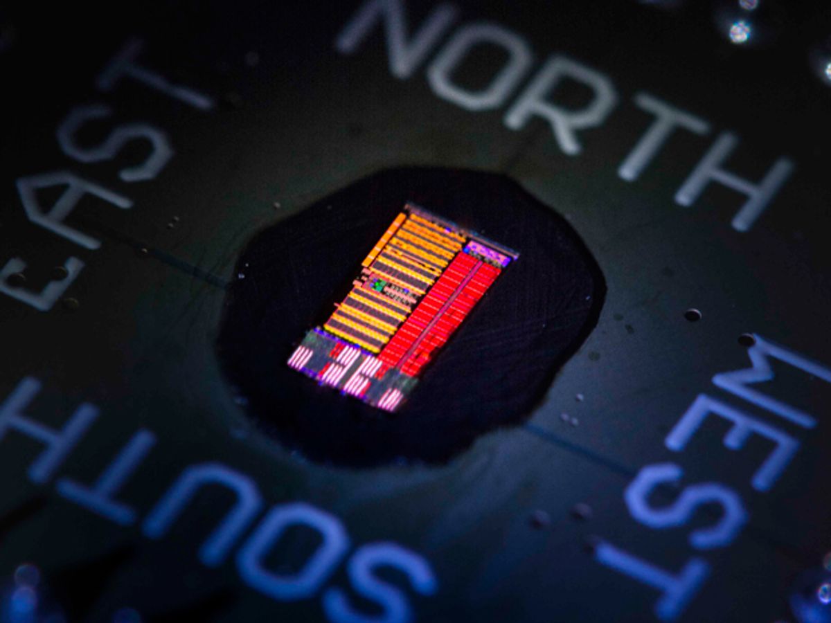
Computer designers have long fantasized about using light rather than electrons to move data between microprocessors. Such optical interconnects would overcome the bandwidth bottleneck inherent in the wires and take full advantage of the leaps in processor speed. But combining two very different technologies—electronics and photonics—in the same silicon chip has been a high hurdle to overcome.
Now a group of researchers has come up with a way to build huge numbers of silicon transistors and optical components on the same chip, doing so for the first time, without a major overhaul of the chipmaking process. And they used it to build an IC containing 70 million transistors and 850 photonic components, which together provide all the logic, memory, and interconnection functions a processor needs.
In tests that linked two such chips—one acting as the processor, the other as memory—the optical interconnect could pass data at 2.5 gigabits per second in each direction along an optical fiber using a single wavelength of light, supplied by an external laser. Adding bandwidth is as simple as adding more wavelengths. Although they did not test it to this extreme, the chip should have been able to transfer 27.5 Gb/s in each direction through the same fiber.
The engineers involved—from MIT, the University of California, Berkeley, and the University of Colorado Boulder—invented what they call their “zero-change” approach to chipmaking. It relies on the standard CMOS processes used to make today’s computer chips—specifically a high-performance process for the so-called 45-nanometer node, which debuted in 2007. “We didn’t make any changes to the process,” says MIT’s Chen Sun.
They started with a silicon substrate; then they added a 200-nm-thick layer of silicon oxide, which acted as an insulator. Over that was the active layer—100 nm of crystalline silicon—plus a 100-nm layer of nitrides and a dielectric coating. The crystalline silicon included a small
amount of germanium to produce strain on the silicon and speed up the circuits.
“We are able to use those existing layers to make our processors,” Sun says. The processor they constructed was based on a dual-core RISC-V architecture—an open instruction set architecture originally developed at Berkeley. It also included 1 megabyte of static RAM.
Key to the process was that some of the silicon substrate was etched away. Because the oxide layer was so thin, the light would have passed through it to the silicon substrate, which would carry it away. Removing the substrate reduced that loss. The lack of silicon also allowed them to deliver light from an external laser to power the optical components, even though the chip was bonded face down to the printed circuit board. But etching couldn’t be done across the entire chip. The team left the silicon in place under the microprocessor and memory, where no light is coming out anyway, so they could attach a heat sink to keep the processor cool.
The real heart of the photonics portion of the chip was the microring resonator, a loop 10 micrometers across that’s coupled to a waveguide. They doped the structure with the same elements used to make p-n junctions in the transistors, and that action created a notch filter, which passes all incoming light except for a single wavelength. Putting a negative voltage across the junction pushed the charge carriers out of the ring, while a positive voltage returned them, creating a modulator that imprinted digital signals onto the light beam.
While the modulator is the answer to transmitting a light-encoded signal, receiving it and turning it into an electronic signal that the processor can work with requires a photodetector. Here the microring is also important. Normally, a photodetector made of the silicon germanium in the chip would have to be many millimeters to a centimeter long to have a chance of absorbing enough photons to actually detect the light. And that’s way too big. But with the microring resonator it can be much smaller, because the light passes through it so many times that the SiGe can absorb it and generate an electronic signal.
Microring resonators have existed for a while, but “a lot of people in industry kind of ignored them,” says Sun. That’s because as they heat up, the index of refraction shifts and they drift away from the desired wavelength.
The solution was to develop active thermal stabilization. The stabilization system includes a separate photodetector and a digital controller. When the detector notices a change in the amount of photocurrent coming to it, the controller alters the voltage across the microring. This changes how much heat the structure dissipates, pushing its index of refraction back to normal.
Sun says his startup company, Ayar Labs, in Berkeley, hopes to be able to commercialize the technology within a couple of years, but at least one expert is skeptical. Anthony Levi, a professor of electrical engineering and physics in the Photonics Center at the University of Southern California, says the engineers involved in the optoelectronic processor are to be congratulated for making a working chip that integrates photonics and electronics, but he doubts the approach is practical. “The challenges of silicon photonics remain the same as they have always been: This includes too much optical loss, too much power dissipation, too much chip area, and so on,” Levi says.
He says the U.S. Defense Advanced Research Projects Agency, which funded the work, has poured “massive amounts of precious research money” into silicon photonics, but the industry and customers, whose decisions come down to cost, haven’t bought into it. “Even if the technology worked, there has to be a compelling reason to adopt a new and disruptive approach to building systems,” Levi says.
