Neuromorphic computing has so far tried to mimic the synapses between neurons in the brain. But a new approach instead aims to act like dendrites, the spindly structures that branch out from the nucleus of a neuron like the roots of a tree. Dendrites receive signals from other neurons via synapses, transmitting them from tip to stem to the nucleus. In computing, “nanodendrites” could function similarly, according to a team of researchers at Stanford University.
Collaborating with semiconductor manufacturer GlobalFoundries, the researchers proposed one such nanodendrite at the 2023 IEEE International Electron Device Meeting (IEDM) this week. The device, a modified transistor, acts as a switch that detects a sequence of microsecond-long voltage pulses. It turns on, thus allowing current to pass, only if the pulses arrive in the correct order. According to Stanford bioengineering professor Kwabena Boahen, this approach could lead to efficient parallel processing in the 3D chips that AI will increasingly depend upon. By emulating the brain’s dendrites, these chips would use less energy and, importantly, generate less heat.
Heat presents a “fundamental issue” in today’s 3D chip technologies, says electrical engineer H.-S. Philip Wong, an IEEE Fellow and a professor of electrical engineering at Stanford. The heat generated grows in proportion to the volume—but the chips dissipate heat at a rate proportional to surface area. That’s why, currently, “all computational advances are limited by heat dissipation,” Wong says.
The problem can be solved by the nanodendrite approach, Wong suggests, because it uses voltage in discrete pulses instead of continuously held levels. It therefore activates fewer wires at any given moment and thus generates less heat.
A typical field-effect transistor consists of three terminals: the source, gate, and drain. For charge to move from the source to the drain, a voltage is applied to the gate, changing the electric field and the conductivity of the silicon. The Stanford device maintains the same basic elements, but it splits the transistor’s gate into three parts. It also embeds a thin layer of ferroelectric material in the multi-part gate, causing polarization to switch when an electric field is applied.
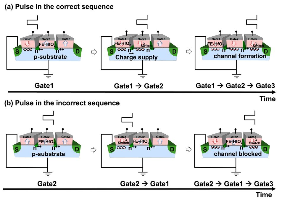 ‘Dendocentric learning’ circuits differentiate between pulses in a correct vs. incorrect sequence. For the former, the switch flips and current is allowed to pass.Stanford University/GlobalFoundries
For charge to move through the channel of the transistor, a series of voltage pulses must be delivered in the right order, starting from the section closest to the source. After the first gate section receives a pulse, charge carriers flow from the source to this section and its polarization flips. The next pulse does the same in the middle section, which draws charger carriers from the first section. Then the third section receives a pulse, completing the conducting channel.
But that won’t happen if the pulses are out of sequence. For example, if a pulse is sent to the middle section of the gate first, followed by the section closest to the source, the middle section won’t be able to draw charge carriers from its neighboring sections. Its polarization will remain the same, hindering the formation of a conducting channel.
Because this type of computing relies on a time-dependent sequence of pulses, “we needed a device that could remember the sequence of pulses,” Wong says. That’s why he and Boahen based the design on ferroelectric transistors, which have previously been proposed as a way of combining memory and logic in neuromorphic chips. The ferroelectric material provides memory in its polarization, which flips when the gate receives a voltage pulse; it then maintains that polarization until it receives another pulse, explains Hugo Chen, a doctoral student who is advised by Wong and presented the paper at IEDM on Monday.
While the current version of the device presented includes a 3-part gate—the simplest version of a dendrite-like structure—the Stanford team aims to introduce further segmentation in the future. Adding more gate partitions increases resistance, Chen notes, though this is unlikely to be an issue since the devices will be built to enable parallel processing.
Building the 3D devices will also require new processes. These chips, for example, would need to be fabricated at a low temperature, Wong says, adding that “how to build a system like that in 3D is still a pertinent research question.”
- Ferroelectric Semiconductors Could Mix Memory and Logic ›
- Dendrocentric AI Could Run on Watts, Not Megawatts ›