The Conversation (0)

Illustration: Anatomy Blue
Green
In the early 2000s, the commercialization of CMOS image sensors led to smaller and smaller—and cheaper and cheaper—digital cameras. Now the thinnest of mobile phones contains at least two camera modules, and all except the most dedicated photographers have stopped carrying a separate camera, concluding that the camera sensors in their phones take pictures that are good enough.
But do they? In bright sun, parts of an image are often washed out. In low light, images become grainy and unclear. Colors do not quite pop like those taken with a professional camera. And those are just the problems with cameras that record visible light. Although it would be great to have night vision in our cameras, infrared sensors cost a lot more for much poorer image quality than their visible-light brethren.
It's time for another revolution in imaging technology. This one will be brought to you by the quantum dot, a nanometer-size particle of semiconductor material, which acts much differently from its bulk counterpart.
When a semiconductor material absorbs light, it releases an electron from a chemical bond, and that electron is free to roam. The same process happens in a quantum dot (QD). But one thing is different: Although an electron is indeed released, it can't roam as easily; it gets squeezed by the edges of the particle, because the quantum dot is only a few nanometers in diameter. This squeeze is called quantum confinement, and it gives the particle some special properties.
The most useful property for imaging is that the light absorbed by the quantum dot is tunable—that is, the color can be continuously adjusted to almost any wavelength in the visible and infrared spectrum simply by choosing the right material and the right particle size. This tunability works in reverse as well—the color of the light emitted when the electron recombines can be selected precisely. It is this light-emission tunability that in recent years inspired the manufacturers of TVs and other kinds of displays to use quantum dots to improve color reproduction. (They've given the enhancement a number of names; the most common branding is “QLED.")
In addition to tunability, quantum dots have a few other nice features. Their small size allows these particles to be incorporated into printable inks, making quantum dots easy to slip into a manufacturing process. Quantum dots can absorb light more efficiently than silicon, which could allow camera makers to produce thinner image sensors. And QDs are sensitive across a broad dynamic range, from very low light to very high brightness.
Before we tell you how quantum-dot cameras will work—and when they will likely be commercially available—we should explain something about the CMOS sensor, today's state of the art for digital images. Clearly there has been considerable progress in the underlying technology in the past decade or two, particularly in making it smaller and cheaper. But the way in which it converts light into an image has largely remained unchanged.
In a typical camera, like the one in your phone, light passes through a series of lenses and a mosaic of red, green, and blue filters before being absorbed by one of the sensor pixels (sometimes called a photosite, to distinguish it from a pixel on an image) on the silicon CMOS chip. The filters determine which color each photosite will record.
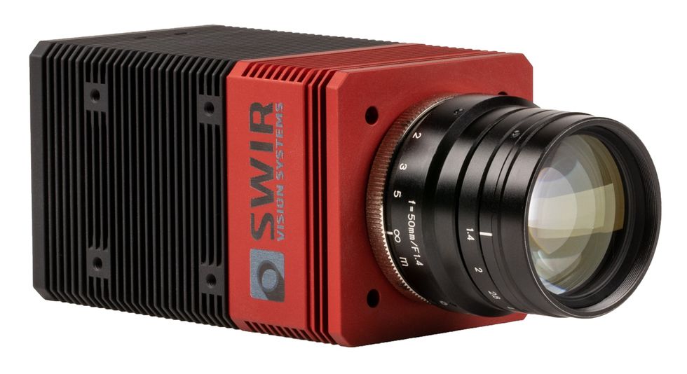 Quantum Dots on Board: The Acuros from SWIR Vision Systems is the first commercially available infrared camera to use quantum-dot-based image sensors, giving it a cost advantage over traditional infrared cameras.Photo: SWIR Vision Systems
When a photosite absorbs a photon, an electron is freed from a chemical bond and moves to an electrode at the edge of the pixel, where it is stored in a capacitor. A readout circuit converts the charge collected in each photosite over a set time to a voltage. The voltage determines the brightness for that pixel in the image.
A common manufacturing process creates both the silicon detectors and the readout circuits. This process involves a long but well-established series of steps of photolithography, etches, and growths. Such fabrication keeps costs low and is relatively simple. But it saddles silicon detectors with some disadvantages.
Typically, the readout electronics go on top of the detector, in what are called front-illuminated devices. Because of this placement, the metal contacts and traces reflect some of the incident light, decreasing efficiency. Back-illuminated devices avoid this reflection by having the readout electronics under the detector, but this placement increases fabrication cost and complexity. Only in the last decade has the cost of back-illuminated sensors dropped enough for them to be used in consumer devices, including phones and digital cameras.
Finally, silicon absorbs only wavelengths less than about 1 micrometer, so it won't work for imaging beyond the near-infrared range.
Now let's look at how quantum dots can change this equation.
As we mentioned before, by precisely tailoring the size of quantum dots, manufacturers of the materials can select exactly what wavelengths of light they absorb. The largest quantum dots in the visible spectrum, about 10 nanometers in diameter, absorb ultraviolet (UV), blue, and green light, and they emit red light, which is to say they're fluorescent. The smaller the QD, the more its absorption and emission shift toward blue in the color spectrum. For example, cadmium selenide QDs of about 3 nm absorb UV and blue light and emit green light.
Cameras with quantum-dot–based detectors operate basically the same way as their silicon CMOS counterparts. When a QD in a photosite absorbs a photon, an electron escapes its localized bond. The edge of the QD confines the electron's travels. However, if another QD is close enough, the free electron can “hop" over to it and, through sequential hops between QDs, reach the photosite's electrode where it can be counted by the pixel's readout circuit.
The readout circuits are manufactured in the same way as those built for silicon photodetectors—fabricated directly on a wafer. Adding the quantum dots to the wafer does add a processing step but an extremely simple one: They can be suspended in a solution as a sort of ink and printed or spin-coated over the circuitry.
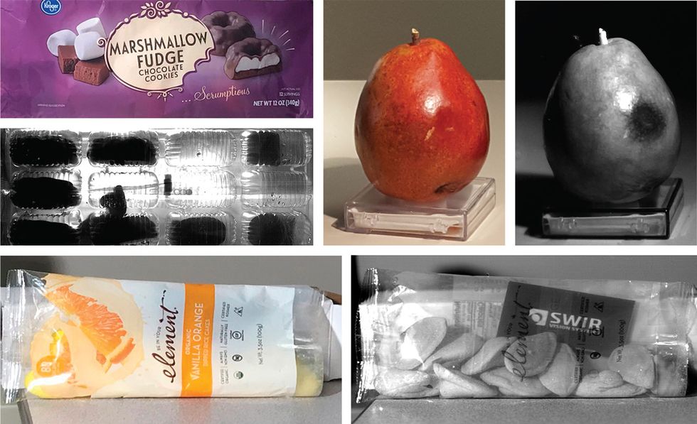 Infrared Vision: Commercial applications of quantum-dot infrared cameras include quality control and food sorting. In these images, a standard CMOS visible-light sensor was used to record the full-color images; an Acuros infrared camera equipped with quantum-dot technology captured the monochrome images.Photos: SWIR Vision Systems
Made in this way, quantum-dot photodetectors have the performance advantage of back-illuminated pixels, where nearly all the incident light reaches the detectors, without that technology's added cost and complexity.
And quantum dots have another advantage. Because they absorb light better than silicon, it takes only a thin layer atop the readout circuitry to gather almost all of the incoming photons, meaning the absorbing layer doesn't need to be nearly as thick as in standard CMOS image sensors. As a bonus, this thin, highly absorbing layer of QDs excels in both low light and high brightness, giving the sensor a better dynamic range.
And, as Steve Jobs used to say, “there's one more thing." Quantum-dot–based cameras have huge potential to bring infrared photography mainstream, because their tunability extends into infrared wavelengths.
Today's infrared cameras function just like visible-light cameras, although the materials used for light absorption are quite different. Traditional infrared cameras use semiconductors with a small bandgap—such as lead selenide, indium antimonide, mercury cadmium telluride, or indium gallium arsenide—to absorb light that silicon does not. Pixel arrays made from these materials must be fabricated separately from the silicon CMOS circuits used to measure currents and generate an image. The detector array and circuit must then be connected at every pixel, typically by metal-to-metal bonding.
This time-consuming process, also known as hybridization, involves putting a small bump of low-melting-point indium on every pixel of both the detector array and the CMOS circuitry. The manufacturing machinery must then line the two up and press them together, then briefly melt the indium to create electrical connections. The complexity of this process limits the possible array sizes, pixel sizes, and sensor resolutions. Worse still, because it's done one camera chip at a time, hybridization is a low-throughput, costly process.
But quantum dots that are just as sensitive to infrared light as these traditional materials can be synthesized using inexpensive, large-scale chemical processing techniques. And, just as with their visible-light cousins, infrared-absorbing QDs can be painted onto chips after the silicon circuitry is complete, a quick and easy process needing no hybridization. Eliminating hybridization means that the resolution—the pixel size—can be less than the 15 µm or so needed to accommodate indium bumps, allowing for more pixels in a smaller area. A smaller sensor means smaller optics—and new shapes and sizes of infrared cameras at a far lower cost.
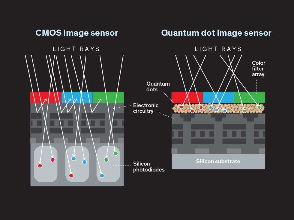 QD or Not QD: A quantum-dot image sensor for visible light (right), has several advantages over traditional CMOS technology (left), including its relative thinness, its elimination of reflections that prevent photons from being received, and the reduction of filtering errors caused by photons being received by the wrong photodiode.Source: Invisage
All these factors make quantum dots seem like a perfect imaging technology. But they aren't without challenges. Right now, the main obstacles to commercialization are stability, efficiency, and uniformity.
Manufacturers mainly solved these issues for the light-emitting quantum dots used in television displays by developing scalable chemical processes that enable the creation of high-efficiency dots in large quantities with very few defects. But quantum dots still oxidize in air, causing imperfections and changes to the sensor properties, including reduced sensitivity, increased noise, slower response time, and even shorting.
This stability problem didn't get in the way of commercialization of displays, however, because protecting the QDs used there from the atmosphere isn't terribly difficult. In the way that QDs are currently used in displays, the QD absorbs light from a blue LED and the photogenerated charge carriers stay within each individual quantum dot to recombine and fluoresce. So these QDs don't need to connect directly to circuitry, meaning that they can be protected by a surrounding polymer matrix with a barrier layer added on both sides of the polymer film, to prevent atmospheric exposure.
But for use in photodetection, sealing off individual QDs in a polymer won't work: The ejected electrons need to be free to migrate to the electrodes, where they can be counted.
One approach to allowing this migration while protecting the QDs from the ravages of the atmosphere would be to encapsulate the full layer of QDs or the entire device. That will likely be the initial solution. Alternatively, the QDs themselves could be specifically engineered to reduce the impact of oxidation without creating a barrier to charge transport, all while maintaining stability and processibility. Researchers are working toward that goal, but it's a tall order.
Another hurdle comes from the organic surfactants used today to maintain a stable solution of the quantum dots. These surfactants act as insulators, so they keep charge carriers from moving easily through the film of QDs to the electrode that collects the signal. Right now, manufacturers deal with this by depositing the QDs as a thin film and then replacing the long surfactant molecules with shorter ones that increase conductivity. But this adds a processing step and can make the QDs more susceptible to degrading over time, as the replacement process can damage the outer layer of QDs.
There is also a problem with the efficiency of photon detection. Due in part to their small size and large surface area, quantum dots can have many defects— imperfections in their crystal lattices that can cause photogenerated charges to recombine before the electron can reach an electrode. When this happens, the photon that initially hit the quantum dot is never detected by the circuitry, reducing the signal that ultimately reaches the camera's processor.
In traditional photodetectors—ones that contain single-crystal semiconductors—the defects are few and far between, resulting in efficiencies of greater than 50 percent. For QD-based photodetectors, this number is typically less than 20 percent. So in spite of the QDs themselves being better than silicon at absorbing light, the overall efficiency of QD-based photodetectors can't yet compete. But quantum-dot materials and device designs are improving steadily, with their efficiency continually getting better.
Because manufacturers use chemical processes to make quantum dots, there is some inherent variation in their size. And because the optical and electronic properties of a QD are driven by its size, any deviation from the desired diameter will cause a change in the color of light absorbed. With variations in the source chemicals, along with those in synthesis, purification, and storage, there can be significant size differences between one batch of QDs and another. The manufacturers must control their processes carefully to avoid this. Major companies with experience in this area have gotten quite good at maintaining uniformity, but smaller manufacturers often struggle to produce a consistent product.
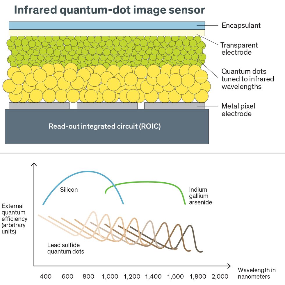 Why Dot? Manufacturability and tunability are among the advantages quantum-dot image sensors can claim over their CMOS counterparts. In the upper diagram, a cross section of SWIR Vision Systems' infrared image sensors shows a group of three pixels. The lower diagram shows the broad range of wavelengths of light that can be received by appropriately tuned quantum dots.Sources: Top: SWIR Vision Systems; Bottom: Sensors, 2017
In spite of these challenges, companies have begun commercializing QD-based cameras, and these products are on the road to becoming mainstream.
A good early example is the Acuros camera, available from SWIR Vision Systems. That company is focused on manufacturing shortwave infrared quantum-dot cameras for use in applications where existing infrared cameras are too expensive. Its camera uses lead sulfide quantum dots, which absorb visible through shortwave infrared light. The detector in this camera currently has an average efficiency of 15 percent for infrared wavelengths, meaning that 15 percent of the photons that hit the detector end up as measurable signal. This is considerably lower than the efficiency of existing indium gallium arsenide technology, which can reach 80 percent. But with 15-µm pixels, the Acuros camera has a higher resolution than most infrared cameras. And it's sold at a price that, the company indicates, should be attractive to commercial users who cannot afford a traditional infrared camera—for applications like maritime imaging, produce inspection, and industrial-process monitoring.
As for the consumer camera market, in 2017 TechCrunch reported that Apple had acquired InVisage, a company dedicated to creating quantum-dot cameras for use in smartphones. Apple, as usual, has been quiet about its plans for this technology.
It may be that Apple is more interested in the infrared capabilities of QD-based cameras than their visible-light performance. Apple uses infrared light and sensors in its facial recognition technology, and cheaper chips with higher resolution for this purpose would clearly interest the company.
Other companies are also pushing hard to solve the stability and efficiency problems with quantum-dot photo sensors and to extend the boundaries of what is possible in terms of wavelength and sensitivity. BAE Systems, Brimrose, Episensors, and Voxtel are among those working to commercialize quantum-dot camera technology. Academic groups around the world are also deeply involved in QD-based sensor and camera research, including teams at MIT, University of Chicago, University of Toronto, ETH Zurich, Sorbonne University, and City University of Hong Kong.
Within five years, it's likely that we will have QD-based image sensors in our phones, enabling us to take better photos and videos in low light, improve facial recognition technology, and incorporate infrared photodetection into our daily lives in ways we can't yet predict. And they will do all of that with smaller sensors that cost less than anything available today.
This article appears in the March 2020 print issue as “Snapshots by Quantum Dots."


