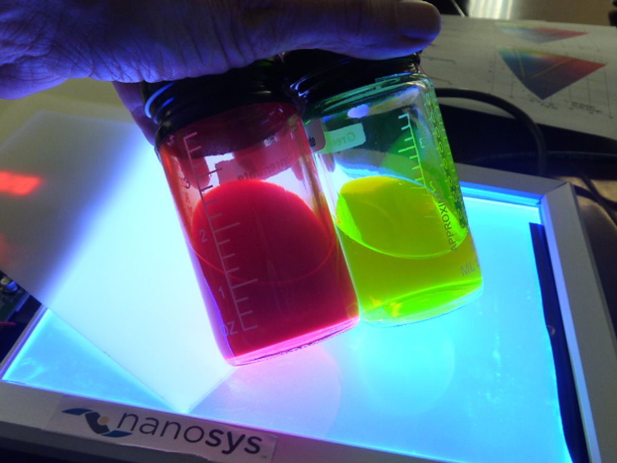
Next month, Samsung’s first Quantum Dot televisions begins shipping to consumers; Hisense plans to start rolling quantum dot televisions off its manufacturing lines mid-year, and other TV manufacturers, including TCL, Skyworth, ChangHong, Sharp, and LG also have unveiled quantum dot TVs that will likely come to market soon. Sony introduced a version of the technology in 2013.
Quantum dots, nanoscale semiconductor crystals, turn blue light into narrow-spectrum greens and reds. It’s these narrow wavelengths of light that allow quantum dots to make traditional LED screens produce the brighter and wider range of colors that make quantum dot televisions stand out. (More on how that works here.) But before quantum dots can create brilliant colors, someone has to make the quantum dots. A few companies are doing so, either using their own or licensed technology, including Nanoco, QD Vision, Quantum Materials, and Nanosys. Turns out one of those is doing its manufacturing here in Silicon Valley.
Nanosys, founded in 2001, is making more than 80 sextillion quantum dots a month in a manufacturing facility in Milpitas—that’s a little over 2 tons of the quantum dot material in a concentrated slurry. It also licensed its manufacturing technology for use by Samsung in production facilities in Korea, and will be opening another plant in the United States, at an as yet unannounced location, later this year.

I recently took a walk through that Milpitas factory, the first journalist to do so, Nanosys CEO Jason Hartlove told me. And while I wasn’t allowed to take pictures of the manufacturing operations themselves, I can tell you what I saw.
First, a little background. Right now there are two competing approaches to getting quantum dots into an LED TV. One uses tubes of quantum dots placed at the edges of the screen, the other uses a film of quantum dots placed across the back of the screen. Nanosys’s quantum dots are used in the film approach; the company ships its red and green quantum dots, diluted in a clear epoxy resin, to 3M and LMS Global for spreading onto a thin plastic film that scatters light; it calls this QDEF, or Quantum Dot Enhancement Film.
A couple of things that struck me.
—Quantum dots are small. Really small. Of course I know that that is true with all nanomaterials, but I don’t think I really got that until seeing these two vials (top photo): each contains approximately 1019 quantum dots, Hartlove told me. Quantum dot film uses billions of the particles per square inch.
—The light these particles produce is strikingly pure. Yes, again, duh, I knew that. But I didn’t KNOW that until Hartlove pulled out his spectrometer. Take a look at the video below of the demo that made this concept a bit clearer.
—Different cultures have different tastes in light. Because quantum dots are produced separately and then combined, Nanosys can vary the blend to create, say, the cooler, bluer light popular in Japanese-made televisions or the warmer, redder light Apple likes for the screens on its mobile devices

—The whole process looks a lot like brewing beer—and the dots go out the door in pony kegs. (Well, the canisters looked a lot like pony kegs.)
More on that process: In about half a dozen large metal tanks—nearly the size of those you might see in a brewpub, not a giant commercial brewery—Nanosys combines cadmium and selenium and adjusts the temperature, concentration, and catalysts added to force these precursors to combine into stable crystals of cadmium selenide. Then, by readjusting the conditions, the system stops the formation of crystals and triggers the beginning of crystal growth. A computer controls the process according to a programmed “recipe;” staff members monitor the growth of the crystals by shining light on them and measuring the wavelength of the fluorescence; the smallest crystals don’t fluoresce at all, then, as the crystals get larger, the wavelength changes. Nanosys stops the process when the fluoresced light hits the target wavelength, which varies depending on what particular display industry standard that the batch of film is designed to meet. For example, for a film that would meet the new color standard for Ultra High Definition (UHD) broadcasts that would be a 640-nm red and a 525-nm green wavelength. After crystal growth stops, the system evaporates the solvent that enabled the dots to easily flow through the brewing equipment, and mixes the remaining material with an epoxy slurry before pouring it into small kegs for shipping.
This is the standard process, which has one major drawback—cadmium is a toxic metal, and, while the tanks and pipes of the manufacturing operation are sealed and environmentally safe—exceeding, Hartlove says, all environmental and safety requirements—it’s harder to control disposal of the TVs years later. That’s why the quantum dot manufacturers like Nanosys are also making cadmium-free quantum dots, out of indium and phosphorous. Nanosys has a second manufacturing line currently dedicated to that cadmium-free technology, though the company says each line could be easily moved to the alternate approach.

To date, cadmium-free quantum dots aren’t universally used, Hartlove explained, because they are harder to produce precisely and therefore don’t perform as well. The color of a quantum dot is determined by the size of the crystal and the band gap of the material; the lower the band gap, the smaller the crystal needs to be to produce a particular color. And when you make crystals smaller, the manufacturing process has to be that much more precise. Says Hartlove, “The impact of 5 atoms more or less on a crystal of 400 atoms is much different than on a crystal of 200 atoms.” The cadmium-free crystals of indium and phosphorus Nanosys is working with now are between 8 and 40 atoms across compared with between 10 and 50 atoms across for its cadmium-selenium crystals. The spectral width of the light they produce is just under 40 nm wide, not as narrow as the sub-30 nm range of the best cadmium selenide quantum dots, Hartlove says, which means that they are less efficient when used in a display system.
Nanosys’ Milpitas operation, though it may be manufacturing huge numbers of quantum dots, is not a huge facility, and the manufacturing operation only takes about a dozen people per shift to operate. I saw one of two manufacturing areas; it was about the size of a large classroom; the other line, I was told, is about the same size. But again, the materials being produced are small, and, Hartlove says, the company can make enough quantum dots for 6 million 60-inch television displays annually from this facility.
And that’s why, Hartlove says, it’s the perfect type of product to manufacture in Silicon Valley.
“This is the promise of nanotech,” Hartlove says. “When you leverage chemistry for self-assembly, the labor cost is negligible; the key costs are the materials and the IP in designing the molecules and the process.” Nanosys has more than 200 patents granted and more pending, Hartlove says, but the manufacturing know-how can be just as important, and not patentable.
So that’s another reason to keep manufacturing close to home: to keep tight reigns on that knowledge.
Says Hartlove: “This is not a labor game. This is not a China game. This is a know-how game.”
Tekla S. Perry is a senior editor at IEEE Spectrum. Based in Palo Alto, Calif., she's been covering the people, companies, and technology that make Silicon Valley a special place for more than 40 years. An IEEE member, she holds a bachelor's degree in journalism from Michigan State University.


