Now wafer manufacturer Soitec hopes to help them along. On Monday, the firm announced it aims to produce wafers with a structure that could let fabs build 3-D transistors (often called FinFETs) in fewer steps than are needed to create the transistors on an ordinary wafer.
It's a somewhat unexpected move. For a few years now, the Bernin, France-headquartered company has been perfecting a way to build wafers for the FinFET's main competitor: the ultrathin body silicon-on-insulator or fully depleted SOI transistor. The idea behind that device is simple: instead of wrapping a gate around three sides of a 3-D channel to better control the transistor, you simply make the channel of an ordinary planar transistor very thin. This lets the gate "fully deplete" the channel, removing all the free charges and lowering how much current leaks through the device when it's supposed to be off. (FinFET coinventor Chenming Hu devised an excellent garden hose analogy to describe the basics, and the two approaches were covered in detail in IEEE Spectrum's November 2011 feature Transistor Wars)
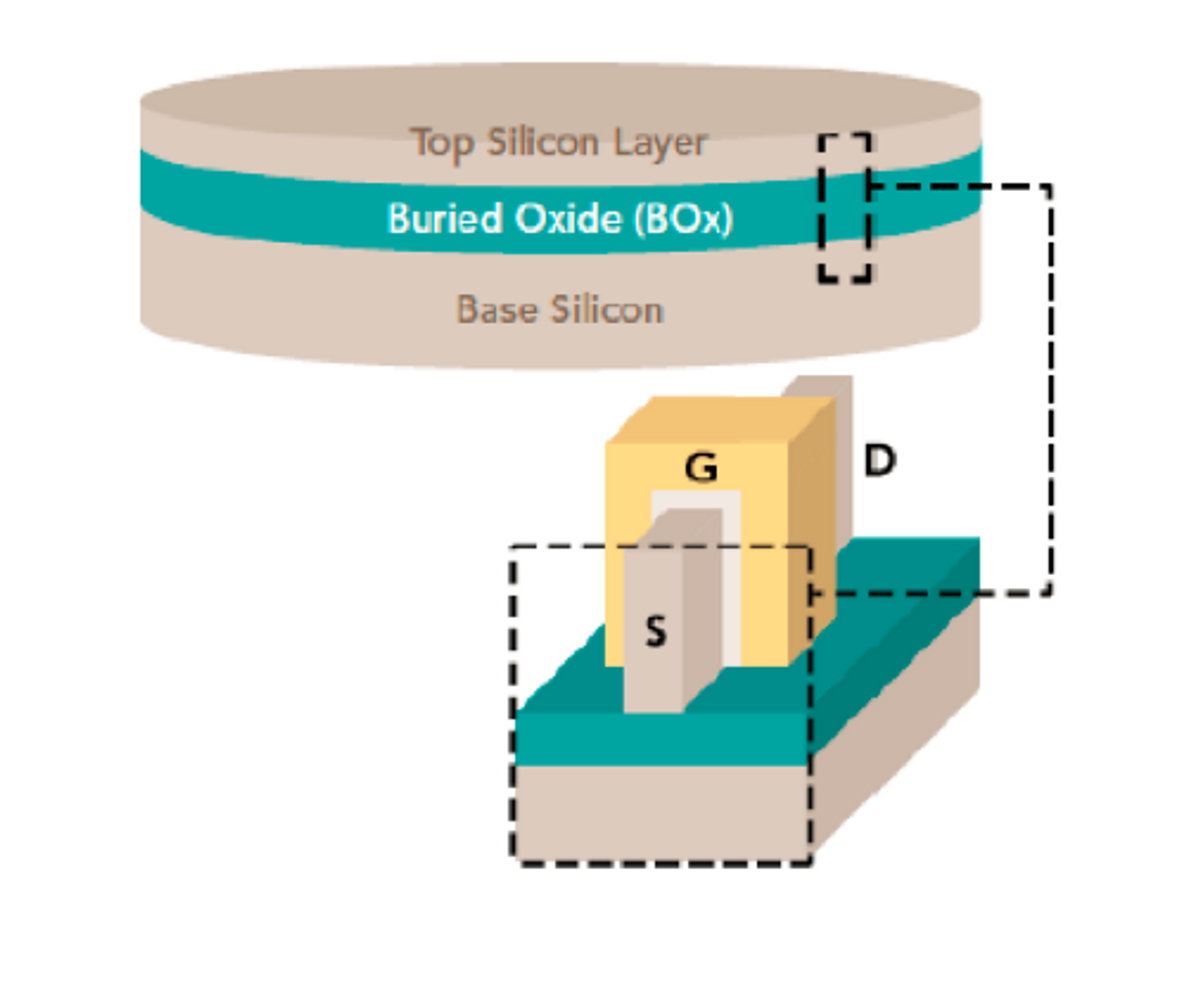
Soitec's FD-2D (for fully depleted, two-dimensions) wafers come with a built-in thin channel -- a silicon layer that can be as thin as 5 nanometers, which sits on top of an electrically insulating layer of buried oxide, which itself sits on a thicker silicon wafer for stability. The wafers are made by implanting ions into a wafer to loosen a thin layer of silicon, which can then be transferred to another wafer.
These 2-D-optimized wafers are already pretty far along. ST-Ericsson, Soitec's first public customer, announced in March that it's picked the technology for future smartphone and tablet chips. Soitec says chips made with their FD-2D wafers see a 40 percent boost in speed or a 40 percent reduction in energy consumption compared to chips made on bulk silicon wafers.
But Soitec envisions its wafers will be useful for more than just extending the life of planar transistors. Steve Longoria, a senior vice president at Soitec, says the company will be ready to start production on a new wafer line, dubbed FD-3D, in 2013. These wafers boast thicker top silicon layers that are designed to form the entirety of the fin in a 3-D transistor structure. Integrating that bit of the transistor-making process into a uniform wafer eliminates one of the big difficulties in the FinFET manufacturing process -- controlling the height of the device. FinFETs made with the wafers will also be more energy efficient, Longoria says, because the bottom of the structure (the only side not controlled by a gate) rests against the buried oxide layer instead of against more silicon, as it would in a traditional chip.
Longoria says the company’s wafers cost about US $500 when bought in volume, compared to $120 for an all-silicon wafer. But Soitec is confident that the extra cost of the wafers can be more than offset by the amount chipmakers will save as a result of fewer manufacturing steps, less variability in chip quality, less investment in tools, and lower materials costs.
Selling chipmakers on more expensive wafers might take some time. There is a “chicken and egg problem of volume and customers,” Longoria admits. The company's new two-pronged approach, aimed at both sides of the coming transistor war, should help on that front.
(Image: IBM)
Rachel Courtland, an unabashed astronomy aficionado, is a former senior associate editor at Spectrum. She now works in the editorial department at Nature. At Spectrum, she wrote about a variety of engineering efforts, including the quest for energy-producing fusion at the National Ignition Facility and the hunt for dark matter using an ultraquiet radio receiver. In 2014, she received a Neal Award for her feature on shrinking transistors and how the semiconductor industry talks about the challenge.


