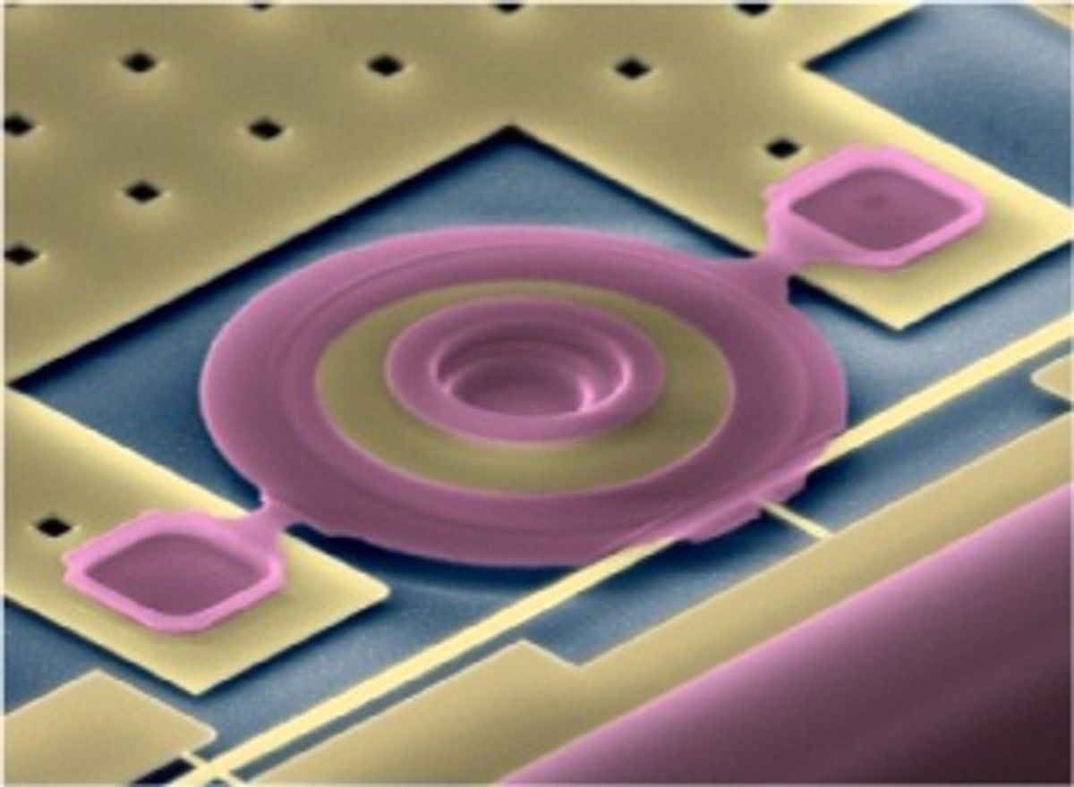
So, in addition to scales that can weigh single protein molecules to an accuracy of a few hundred times the mass of a proton, we now have a position sensor that can detect changes in displacement as small as 1/30,000th of the diameter of a single carbon atom, or about the diameter of a single carbon nucleus.
Houxun Miao, Kartik Srinivasan, and Vladimir Aksyuk (researchers at the National Institute of Standards and Technology’s Center for Nanoscale Science and Technology) have built a microelectromechanical system (MEMS) that pushes the lower limits of distance and force measurement down to within a short hail of the theoretical limits—to 2.3 times the standard quantum limit.
Both silicon and silicon nitride are transparent to infrared light. This means that the Si disk can act as an optical cavity—a photonic hall of mirrors that reflects light almost endlessly around its perimeter. “The light can be trapped inside the disk, close to its outer edge, and travel around in circles inside,” Aksyuk says. “It is trapped the same way at the light is trapped inside optical fibers used for transmitting light over long distances, but here it just goes in circles.” It is, he says, similar to an acoustic whispering gallery, which traps sound along a concave wall.
The key is the “evanescent tail.” Even when light is fully trapped in a channel—a fiber optic cable, a waveguide, or a silicon disk--its wave function extends outside beyond the channel’s borders. That’s the evanescent tail. The NIST device positions three components—the waveguide, the silicon ring, and the silicon nitride disk—close enough together so that their evanescent tails can interact.
The researchers tune light so that its wavelength is an integral fraction of the disk’s circumference. When they pump it from the waveguide (the pipe running from lower left to upper right of the SEM) into the disk, it will resonate in the optical cavity. “Under this condition the optical power inside the disk is increased dramatically—by up to 370,000 times in our case,” Aksyuk says.
Any displacement of the nitride ring changes its interaction with the disk’s evanescent tail (the blue dots at the rim of the disk in the schematic), diverting some of its energy into the ring and reducing the resonance frequency. The researchers read the new resonant mode, and the frequency change indicates the change in displacement.
It’s important to note that, though future versions will likely be cryogenically cooled, the test device operated at room temperature, where thermal noise is a major problem. The NIST group coupled a “cold-damping” loop into the actuator controls, feeding the ring’s noise oscillations back with a phase delay to counteract the jitters. Think of it as the world’s smallest noise-cancelling headphone.
Images: V. Aksyuk, NIST
Douglas McCormick is a freelance science writer and recovering entrepreneur. He has been chief editor of Nature Biotechnology, Pharmaceutical Technology, and Biotechniques.


