
The blue light-emitting diode, arguably the greatest optoelectronic advance of the past 25 years, harbors a dark secret: Crank up the current and its efficiencies will plummet. The problem is known as droop, and it’s not only puzzling the brightest minds in the field, it’s also threatening the future of the electric lighting industry.
Tech visionaries have promised us a bright new world where cool and efficient white LEDs, based on blue ones, will replace the wasteful little heaters known as incandescent lightbulbs. More than a dozen countries have already enacted legislation that bans, or will soon ban, incandescent bulbs. But it’s hard to imagine LEDs dislodging incandescents and coming to dominate the world electric lighting industry, unless we can defeat droop.
In flashlights, in backlights for screens in cellphones and now televisions, and in a bunch of other applications, white LEDs already constitute a multibillion-dollar market. But that’s just a US $5 billion niche compared to the overall lighting industry, whose sales next year should reach $100 billion, according to the market research firm Global Industry Analysts. The trick will be to make LEDs turn electricity into light efficiently enough to offset their relatively high cost—roughly 16 cents per lumen, at lightbulb-type brightness, as opposed to about 0.1 cents or less for incandescents.
Look at the competition and you’d think the job was easy. Today’s garden-variety incandescent bulbs aren’t much different from the ones Thomas Edison sold more than a century ago. They still waste 90 percent of their power, delivering roughly 16 lumens per watt. Fluorescent tubes do a lot better, at more than 100 lm/W, but even they pale next to the best LEDs. The current state-of-the-art white LED pumps out around 250 lm/W, and there’s no reason why that figure won’t reach 300 lm/W.
Unfortunately, these LEDs perform at their best only at low power—the few milliamps it takes to backlight the little screen on your mobile phone, for instance. At the current levels needed for general lighting, droop kicks in, and down you go, below 100 lm/W.
The first-ever report of light emission from a semiconductor was by the British radio engineer Henry Joseph Round, who noted a yellowish glow emanating from silicon carbide in 1907. However, the first devices at all similar to today’s LEDs arrived only in the 1950s, at Signal Corps Engineering Laboratories, at Fort Monmouth, in New Jersey. Researchers there fabricated orange-emitting devices; green, red, and yellow equivalents followed in the ’60s and ’70s, all of them quite inefficient.
The great leap toward general lighting came in the mid-1990s, when Shuji Nakamura, then at Nichia Corp., in Tokushima, Japan, developed the first practical bright-blue LED using nitride-based compound semiconductors. (Nakamura’s achievement won him the 2006 Millennium Technology Prize, the approximate equivalent in engineering of a Nobel Prize.) Once you’ve got blue light, you can get white by passing the blue rays through a yellow phosphor. The phosphor absorbs some of the blue and reradiates it as yellow; the combination of blue and yellow makes white.
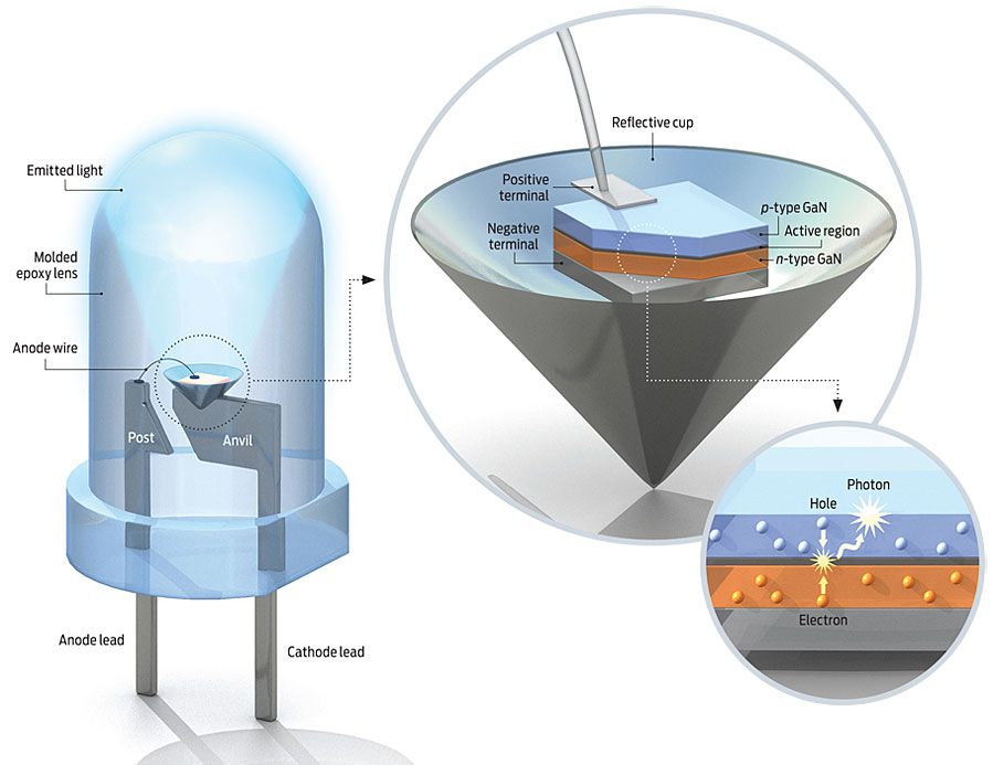
All LEDs are fabricated as aggregated sections, or regions, of different semiconductor materials. Each of these regions plays a specific role. One region serves as a source of electrons; it consists of a crystal of a compound semiconductor into which tiny amounts of an impurity, such as silicon, have been introduced. Each such atom of impurity, or dopant, has four electrons in its outer shell, compared with the three in an atom of gallium, aluminum, or indium. When a dopant takes a place that one of these other atoms would normally occupy, it adds an electron to the crystalline lattice. The extra electron moves easily though the crystal, acting as a carrier of negative charge. With this surfeit of negative charges, such a material is called n-type.
At the opposite end of the LED is a region of p-type material, so called because it has excess positive-charge carriers, created by doping with an element such as zinc or magnesium. These metals are made up of atoms with only two electrons in their outer shell. When such an atom sits in place of an atom of aluminum, gallium, or a chemically similar element (from group III in the periodic table), the lattice ends up an electron short. That vacancy behaves as a positive charge, moving throughout the crystal like the missing tile in a sort-the-number puzzle. That mobile vacancy is called a hole.
In the middle of the sandwich are several extraordinarily thin layers. These constitute the active region, where light is produced. Some layers made of one semiconducting material surround a central layer made of another, creating a “well” just a few atoms thick—a trench so confined that the laws of quantum mechanics rule supreme. When you inject electrons and holes into the well by applying a voltage to the n - and p-type regions, the two kinds of charge carriers will be trapped, maximizing the likelihood that they will recombine. When they do, a photon pops out.
To make an LED, you must grow a series of highly defined semiconductor layers on a thin wafer of a crystalline material, called a substrate. The substrate for red, orange, and yellow LEDs is gallium arsenide, which works wonderfully because its atoms are spaced out identically to those of the layers built on top of it. Hardly any mechanical strain develops in the semiconductor’s crystalline lattice during fabrication, so there are very few defects, which would quench light generation.
Unfortunately, blue and green LEDs lack such a good platform. They’re called nitride LEDs because their fundamental semiconductor is gallium nitride. The n-type gallium nitride is doped with silicon, the p-type with magnesium. The quantum wells in between are gallium indium nitride. To alter the light color emitted from green to violet, researchers vary the gallium-to-indium ratio in the quantum wells. A little indium produces a violet LED; a little more of it produces green.
Such LEDs would ideally be manufactured on gallium nitride substrates. But it has proved impossible to grow the large, perfect crystals of gallium nitride that would be necessary to make such wafers. Unipress, of Warsaw, the world leader in this field, cannot make crystals bigger than a few centimeters, and then only by keeping the growth chamber at a temperature of 2200 C and a pressure of almost 20 000 atmospheres.
So the makers of blue LEDs instead typically build their devices on wafers of sapphire, whose crystalline structure does not quite match that of the nitrides. And that discrepancy gives rise to many defects—billions of them per square centimeter.
It is amazing that such LEDs work at all. Any arsenide-based red, orange, or yellow LED that contained as many defects would emit absolutely no light. To this day, researchers, including Nakamura himself—who moved to the University of California, Santa Barbara (UCSB) in 1999—can’t agree on the cause of the phenomenon. Perhaps the solution to this problem may also explain droop.
The explanation won’t come easily. When researchers set out to find the cause of droop in nitride LEDs, one of their first suspects was heat, which they knew could cause droop in arsenide LEDs. There, heat imparts so much energy to the electrons and holes that the quantum well can no longer trap them. Instead of recombining, some of them escape, only to be swept away by the electric fields in the device. But researchers dismissed this possibility after noting that nitride LEDs suffered from droop even when driven by short, pulsed voltages spaced far enough apart to let the devices cool down.
Another theory was proposed as far back as 1996 by Nakamura. He argued that everything could be explained by the structure of the quantum well. Nakamura and his colleagues looked at LEDs with a transmission electron microscope and were surprised to find light and dark areas within the quantum well, suggesting that the material there was not uniform. They then investigated the crystalline structure more closely, using X-ray diffraction, and found that the quantum well had indium-rich clusters (bright) next to indium-poor areas (dark).
Nakamura conjectured that because the indium clusters were free from defects, the electrons and holes would be trapped in them, making bright emission possible, at least at low currents. Continuing with this line of reasoning, Nakamura’s team argued that LEDs’ high efficiency at low currents stemmed from a very high proportion of electron-hole recombination in defect-free clusters. At higher currents, however, these clusters would become saturated, and any additional charge carriers would spill over into regions having defects dense enough to kill light emission. The saturation at high current, they suggested, accounted for the observed droop.
This theory has fallen out of favor in recent years. “To start with, we saw indium-rich clusters in InGaN quantum wells, just as the rest of the world did,” explains Colin Humphreys, the head of the Cambridge Centre for Gallium Nitride at the University of Cambridge, in England. But then he and his team began to suspect that their electron microscope was causing the very thing it was detecting. So the group carried out low-dose electron microscopy. “We looked at the first few frames—a very low exposure—and saw no indium clustering at all. But as we exposed the material to the beam, these clusters developed,” he says. They concluded that the clustering was merely an artifact of measurement.
In 2003, Humphreys presented that jaw-dropping finding at the Fifth International Conference on Nitride Semiconductors, in Nara, Japan. It wasn’t well received. Many delegates contended that something must have gone wrong with the Cambridge samples. So Humphreys’s group went back and studied a wider variety of specimens, including LEDs supplied by Nichia. Their work only reinforced their view that the clusters were formed by electron-beam damage.
In 2007, Humphreys’s Cambridge team, together with researchers at the University of Oxford, described how they had attacked the problem with what’s known as a three-dimensional atom probe. This device applies a high voltage that evaporates atoms on a surface, then sends them individually through a mass spectroscope, which identifies each one by its charge-to-mass ratio. By evaporating one layer after the other and putting all the data together, you can render a 3-D image of the surface with atomic precision.
The resulting images confirmed, again, what the electron microscope had shown: There is no clustering. Discrediting the cluster theory was an important step, even though it left the research community without an alternative explanation for droop.
Then, on 13 February 2007, the California-based LED manufacturing giant Philips Lumileds Lighting Co. made the stunning claim that it had “fundamentally solved” the problem of droop. It even said that it would soon include its droop-abating technology in samples of its flagship Luxeon LEDs.
Lumileds kept the cause of droop under wraps for several months. Then, at the meeting of the International Conference of Nitride Semiconductors, held September 2007 in Las Vegas, it presented a paper putting the blame on Auger recombination—a process, named after the 20th-century French physicist Pierre-Victor Auger, that involves the interaction of an electron and a hole with another carrier, all without the emission of light.
The idea was pretty radical, and it has had a mixed reception. Applied Physics Letters published Lumileds’ paper only after repeated rejections and revisions. “In my experience, it was one of the most difficult papers to get out there,” says Mike Krames, director of the company’s Advanced Laboratories.
Krames’s team used a laser to probe a layer of gallium indium nitride, the semiconductor used for quantum wells in a nitride LED. They tuned the laser to a wavelength that only the gallium indium nitride layer would absorb, so that each zap created pairs of electrons and holes that then recombined to produce photons. When the researchers graphed the resulting photoluminescence against different intensities impinging on the sample, they produced curves that closely fit an equation that described the effects of Auger recombination.
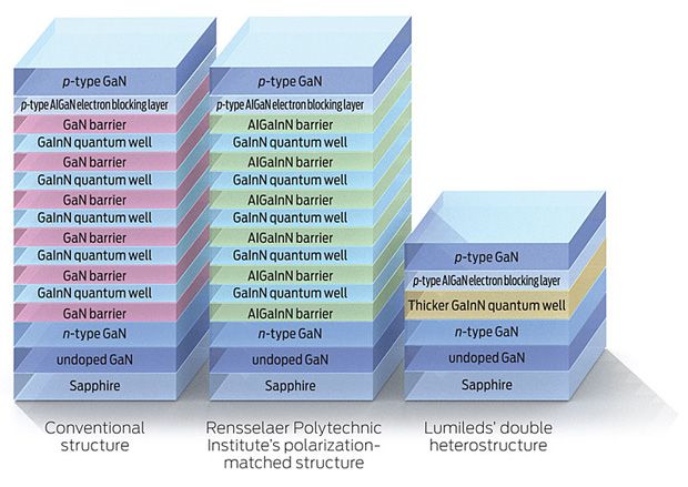
The bad news is that you can’t eliminate this kind of recombination, which is proportional to the cube of the density of carriers. So in a nutshell, if you’ve got carriers—which of course you need to generate light—you’ve also got Auger recombination. The good news, though, is that Lumileds has shown that you can push the peak of your efficiency to far higher currents by cutting carrier density—that is, by spreading the carriers over more material. The company does so with what’s known as a double heterostructure (DH), essentially a quantum well that’s 13 nanometers wide, rather than the usual 3 or 4 nm. It still shows quantum effects, although they are not so pronounced, and the design is less efficient than the standard one at low currents. Still, it excels at higher currents. The Lumileds team has created a test version that delivers a peak efficiency slightly higher than that of a conventional LED.
Promising though this new crystalline structure may be, it is difficult to grow. Perhaps this is why Lumileds has yet to incorporate the design into its Luxeon LEDs. “There are multiple paths to dealing with droop, and we’ve investigated most of these paths,” says Krames. “We have new structures in the pipeline, DH as well as non-DH, and we will move forward with the best structure.”
Not everyone is convinced that Auger recombination is the cause of droop. One such skeptic is Jörg Hader, a University of Arizona theorist, who works with former colleagues in Germany at Philipps-Universität Marburg and at one of the world’s biggest LED manufacturers, Osram Opto Semiconductors, in Regensburg.
“All [Lumileds] showed was that they can fit the results with a dependence that is like Auger,” claims Hader. “It’s a fairly weak argument to see a fit that fits, and see what might correspond to that fitting.” In his view, there’s a good chance that the Lumileds data could also be fitted with other density dependencies, as well as the cubed dependence that is classically associated with Auger recombination.
Hader has calculated the magnitude of direct Auger recombination for a typical blue LED. The equations that describe this interaction of an electron and a hole with a third carrier date back to the 1950s, but that doesn’t mean that they are easy to solve. Hader says he took no shortcuts. Instead, he accounted for all physical interactions in a program tens of thousands of lines long, a program that in its initial form would have taken several years to run. However, Hader says he’s learned what he can omit safely in order to get the running time down to just 1 minute. He says the model shows that Auger losses are too small to account for LED droop, although he does allow that droop might be caused by other processes related to Auger recombination. These processors are more complicated because they also involve defects in the material or thermal vibrations (phonons, in quantum terms) of the semiconductor crystal.
Krames criticizes Hader’s calculations for leaving out the possibility that electrons might occupy higher energy levels, known as higher conduction bands. But Hader believes that including these bands would hardly affect his conclusions.
This May, computer scientists at UCSB brought new evidence to bear on this debate. Chris Van de Walle’s team included a second conduction band in their calculations of Auger recombination in nitrides and concluded that Auger contributes strongly to droop. However, they modeled only the bulk materials, not realistic quantum wells, for which Van de Walle admits his methods cannot handle the calculations, at least not on today’s computers.
Hader does not doubt the general shape of the UCSB results. However, he points out that the value Van de Walle’s team has taken for the second conduction band substantially differs from that given in certain academic papers. Using these published values would have profound effects on any estimate of the magnitude of Auger recombination. The conclusions of Hader and Van de Walle highlight the lack of consensus among theorists over the cause of droop.
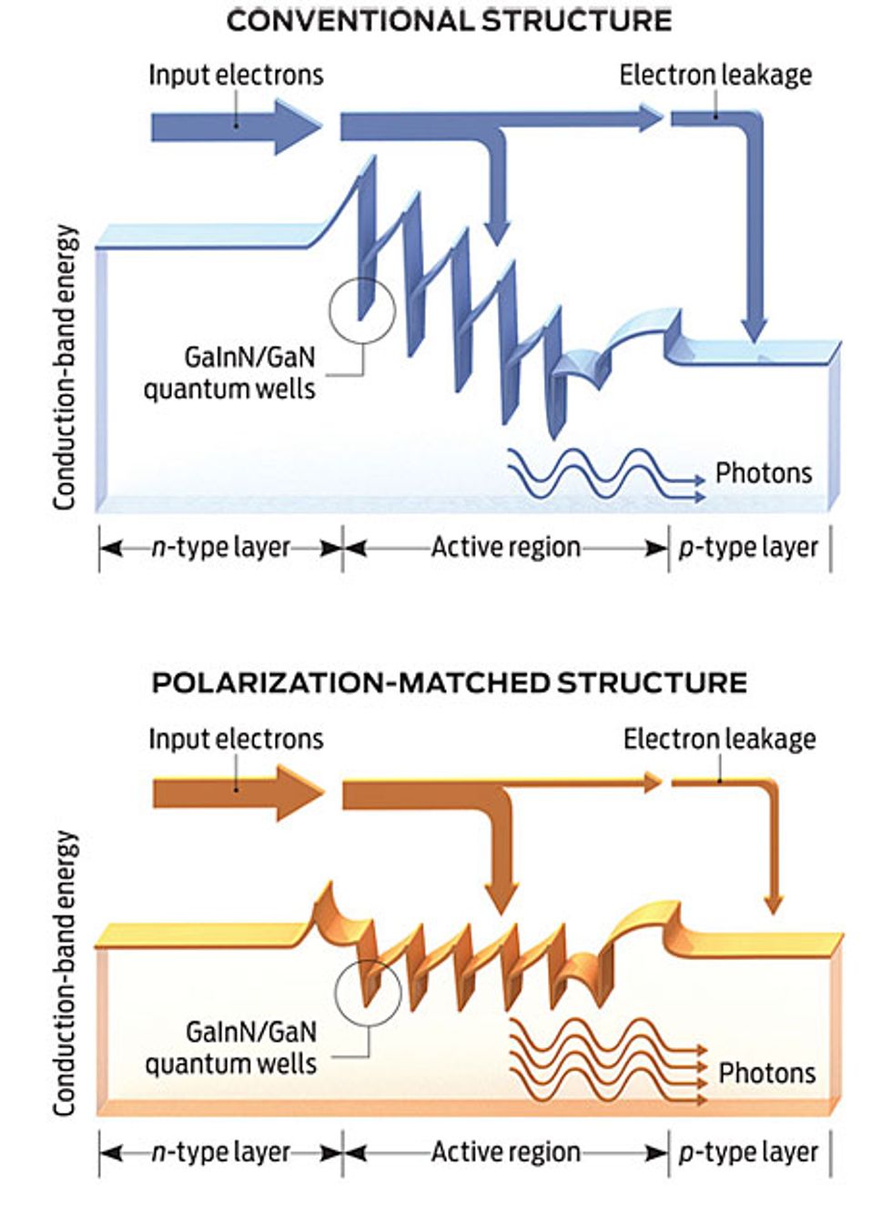 Less Leakage: Polarization fields may cause LED droop. Such fields are claimed to drive electrons out of the active region and into the
p-type layer, where some recombine without emitting light (top). A “polarization matched” structure (bottom) has a far weaker internal field and therefore suffers less electron leakage, leaving more electrons to recombine with holes.Illustration: Bryan Christie Design
Less Leakage: Polarization fields may cause LED droop. Such fields are claimed to drive electrons out of the active region and into the
p-type layer, where some recombine without emitting light (top). A “polarization matched” structure (bottom) has a far weaker internal field and therefore suffers less electron leakage, leaving more electrons to recombine with holes.Illustration: Bryan Christie Design
Meanwhile, a group headed by E. Fred Schubert at the Rensselaer Polytechnic Institute, in Troy, N.Y., has proposed yet another theory. His team, in collaboration with Samsung, blames droop on the leakage of too many electrons from the quantum well.
Interestingly, Schubert’s team, like the researchers at Lumileds, drew its conclusions by pumping light into the nitride structures and observing the light that those structures emitted in response. But Schubert and company investigated full LED structures, and they compared the results they’d obtained from optical pumping with light output generated when a voltage was applied, as it is in normal operation. As expected, droop kicked in when the device was pumped electrically. But the researchers saw no sign of droop in the photoluminescence data.
They then brought in Joachim Piprek, a theorist from the NUSOD Institute, a device simulation consultancy in Newark, Del. He used a computer model to simulate the behavior of a blue LED and found that the strong internal fields characteristic of nitrides must be causing electrons to leak out of the wells.
Now Schubert and his colleagues have produced direct evidence to back up their argument for leakage. They took an LED unconnected to any circuit and hit it with light at a wavelength of 405 nm, which is absorbed only in the quantum wells. The researchers detected a voltage across the diode, implying that carriers must leave the wells, contradicting Lumileds’ theory.
Schubert’s team has tried to control electron leakage by redesigning the LED. By carefully selecting the materials for the active region—switching from the conventional gallium nitride barrier to an aluminum gallium indium nitride version—they have been able to eliminate the charges that tend to form wherever distinct crystalline layers meet. They say such “polarization matching” consistently cuts droop, raising power output by 25 percent at high currents.
Schubert believes that the electrons that leak out of the wells recombine with holes in the p -type region. If he could detect this recombination, it would certainly add weight to his explanation. “We’ve looked for that luminescence,” says Schubert, “but we have not seen it.” He’s not surprised, though, because p -type gallium nitride is a very inefficient light emitter, and the LED’s surface is nearby, so surface recombination at the top contact is also likely.
However, it is possible to detect electrons in the p -type region by modifying the standard LED structure, and researchers at UCSB have done just this. This team, led by Steven DenBaars and Nakamura, did the job of fitting the p -type region with an additional quantum well, one that emits light of a color different from that of the main LED. At a workshop in Montreux, Switzerland, in the fall of 2008, the group reported that they had found just this sort of emission.
Although this experiment proved that electrons do flow into the p -type region, it can’t tell us where they came from. And while Schubert’s theory of electron leakage could explain the results, there may well be other things that can also account for them. We can’t even rule out Auger recombination as the dominant mechanism, because the proportion of electrons flowing into the p -type region is still to be quantified.
Each theory has its champions. Theoreticians at Philipps-Universität Marburg support Auger recombination, mainly the phonon-assisted form, as the main cause of droop. So does Semiconductor Technology Research, a device-modeling company based in Richmond, Va. Meanwhile, Hadis Morkoç’s group at Virginia Commonwealth University seconds Schubert’s support of electron leakage, which they attribute to the poor efficiency with which holes are injected into the quantum well.
Confused? Join the club—and realize that this controversy is precisely what you’d expect to find in a field that has suddenly begun to make great progress. Even if we don’t have a universally agreed-upon theory to account for droop, we do have a growing arsenal of proven weapons to fight it—Schubert’s polarization-matched devices, Lumileds’ wide quantum well structures, as well as designs that improve hole injection, among others. Too bad that we still can’t agree on how they work.
The industry will move forward. LEDs are just starting to supplant fluorescent as well as incandescent lighting. Someday, in our lifetimes, incandescent filaments will finally stop turning tens of gigawatts into unwanted heat. Smokestacks will spew less carbon into the global greenhouse. And we won’t have to get up on stepladders to change burned-out bulbs nearly so often as we do today.
And around that time, when you’re reading this magazine by the light of an LED, perhaps the theorists will have watertight explanations for the experimentalists, and we’ll know the answer to the burning question that remains: What causes droop?
About the Author
Richard Stevenson, author of “The LED’s Dark Secret” [p. 22], got a Ph.D. at the University of Cambridge, where he studied compound semiconductors. Then he went into industry and made the things. Now, as a freelance journalist based in Wales, he writes about them. Between assignments, he builds traditional class A hi-fi amplifiers, as opposed to the class D type favored by IEEE Spectrum’s Glenn Zorpette. “If we were to share an office,” Stevenson says, “many hours would be lost to discussions of the path to hi-fi nirvana.”
To Probe Further
The Philips Lumileds papers are “Auger Recombination in InGaN Measured by Photoluminescence,” by Y. C. Shen, G. O. Mueller, S. Watanabe, N. F. Gardner, A. Munkholm, and M. R. Krames, Applied Physics Letters 91141101, 1 October 2007, and “Blue-Emitting InGaN–GaN Double-Heterostructure Light-Emitting Diodes Reaching Maximum Quantum Efficiency Above 200 A/cm2,” by N. F. Gardner, G. O. Müller, Y. C. Shen, G. Chen, S. Watanabe, W. Götz, and M. R. Krames, APL 91243506, 12 December 2007.
The papers from Rensselaer Polytechnic Institute are “Origin of Efficiency Droop in GaN-Based Light-Emitting Diodes,” by M.-H. Kim, M. F. Schubert, Q. Dai, J. K. Kim, and E. Fred Schubert, J. Piprek, APL 91183507, 30 October 2007; “Effect of Dislocation Density on Efficiency Droop in GaInN/GaN Light-Emitting Diodes,” by M. F. Schubert, S. Chhajed, J. K. Kim, and E. Fred Schubert, D. D. Koleske, M. H. Crawford, S. R. Lee, A. J. Fischer, G. Thaler, and M. A. Banas, APL 91231114, 7 December 2007; and “Polarization-Matched GaInN/AlGaInN Multi-Quantum-Well Light-Emitting Diodes With Reduced Efficiency Droop,” by M. F. Schubert, J. Xu, J. K. Kim, E. F. Schubert, M.-H. Kim, S. Yoon, S. M. Lee, C. Sone, T. Sakong, and Y. Park, APL 93041102, 28 July 2008.
The paper from Jorg Hader, et al., is “On the Importance of Radiative and Auger Losses in GaN-Based Quantum Wells, APL 92261103, 1 July 2008.
The paper from Virginia Commonwealth University is “On the Efficiency Droop in InGaN Multiple-Quantum-Well Blue-Light-Emitting Diodes and Its Reduction with p-Doped Quantum-Well Barriers,” by J. Xie, X. Ni, Q. Fan, R. Shimada, Ü. Özgür, and H. Morkoç, APL 93121107, 23 September 2008.