
9 January 2013—An array of nanometer-scale optical antennas built on a silicon chip holds the promise of holographic televisions and cheaper automobile crash-avoidance systems, its creators say.
Although the concept of such “phased arrays” of antennas—in which the peaks and troughs of a wave from each antenna are combined to send the signal in a particular direction—goes back to the early 20th century for radio waves, recently researchers have been applying it to optics as well. But because optical wavelengths are so much smaller than radio wavelengths, the antennas have to be fabricated with high accuracy, at nanometer scales. So far, that’s kept the arrays small, on the order of 4 by 4 antennas, which are of little use.
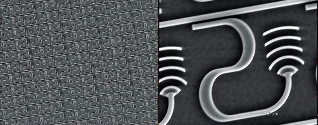
Now Jie Sun, a graduate student, and Michael Watts, an associate professor of electrical engineering, both in the Photonic Microsystems Group at MIT, have used the same fabrication processes that make silicon chips to build a 64- by 64-antenna phased array. Each antenna, which consists of a silicon waveguide and five curved grooves etched in silicon, is 3 micrometers long, 2.8 μm wide, and 0.22 μm thick. The 4096 antennas, each of which constitutes a pixel, fit in a 0.33-square-millimeter area. An infrared laser beam is delivered to the antennas through a waveguide. The researchers describe the device in this week’s issue of Nature .
“We could have gone larger,” Watts says. “We see no reason why you can’t go to extremely large scales. But, of course, that will take quite a bit of development.”
Each antenna’s phase was encoded in the array during fabrication so that the array projected the MIT logo. The real appeal of these advances lies not in such fixed arrays but in arrays where the phase can be shifted so that the antennas can be used to send any desired signal. The team demonstrated a smaller array—64 antennas in an 8-by-8 configuration with doped-silicon heater elements embedded inside the silicon waveguides of each antenna. Running a current through the doped silicon heats the antenna, causing its phase to shift.
An active optical phased array could be used in laser detection and ranging systems, in which a light beam needs to sweep over a target. Such systems could be used in sensors for missile guidance or to quickly detect the position and direction of nearby cars on the highway. Steering a beam with a voltage change rather than a moving mechanical part would be faster and cheaper.
Other possibilities include attaching an array to the end of an optical fiber, which could be inserted into a blood vessel to take an image or deliver a laser beam for surgical procedures. Further down the road, such arrays might be used to build holographic displays, although a display a square meter in size would require controlling 4 trillion pixels, which presents a serious challenge.
Roel Baets, a professor in the Photonics Research Group at Ghent University, in Belgium and the research organization IMEC, whose own graduate student is working on similar arrays, says there are challenges to making practical devices, such as reducing the power requirements, controlling each pixel better, and making the pixels smaller. And Watts says he’d like to move from the infrared band—the work was done at a standard telecommunications wavelength of 1550 nanometers—to the visible, though the shorter wavelengths would require even smaller features and spacing.
Baets says the MIT team is to be commended for demonstrating such a large array, which he called a “nontrivial engineering task.” The fact that it takes advantage of well-established silicon-processing technology makes applications seem more plausible, he says. “This array can be made by a CMOS fab, and that is a big asset,” Baets says.
About the Author
Based in Lowell, Mass., Neil Savage writes about strange semiconductors, unusual optoelectronics, and other things. In December 2012, he reported on technology to turn discarded eggshells into components for supercapacitors.