
It’s the late 1970s, the U.S. economy is reeling from years of sky-high oil prices, and President Jimmy Carter desperately wants to reverse the downward spiral in the nation’s prosperity and morale. Seeking wisdom from the crowd, he brings ordinary citizens to Camp David, who, as he later recounts in his famous “malaise” speech, tell him: “Be bold, Mr. President. We may make mistakes, but we are ready to experiment.”
One person ready to experiment—in the literal sense—was B. Jayant Baliga, the recipient of this year’s IEEE Medal of Honor. At the time, he was developing semiconductor power devices for General Electric, which used countless electric motors in its many products—countless motors that drew countless watts.
Most were induction motors, whose speeds were governed by the power-line frequency. So when a machine required less oomph, there was no good way to slow it down. The usual work-around was to insert a physical barrier into the stream of air or water that was being pumped around. No wonder electric appliances of that generation were atrociously inefficient.
Some GE engineers wanted to pursue a simple energy-saving idea: Just drive the motor at the desired speed. But that required adding electronics to send power to a motor’s windings at variable frequencies, which wasn’t easy to do back then. The voltages were too high for metal-oxide-semiconductor field-effect transistors (MOSFETs) to work efficiently, and ordinary bipolar power transistors required bulky and expensive control and protection circuits.
Facing those difficulties, a GE manager in charge of drives for air conditioners appealed to the company’s researchers. “You guys need to give me some innovation that will make my business succeed,” Baliga recalls him saying.
And that’s exactly what Baliga did. Around 1980, he created the insulated-gate bipolar transistor, or IGBT, which today is found in household appliances, factory robots, fluorescent lights, automobiles, trains, televisions, photovoltaic installations—anywhere modestly high voltages need to be switched on and off quickly.
As influential as it has been, the IGBT is far from Baliga’s only contribution to power semiconductors. Now a professor of electrical and computer engineering at North Carolina State University, in Raleigh, he has spent his career not only pursuing experimental advances but also developing fundamental semiconductor theory, writing textbooks, and laboring in the business trenches bringing devices to market. Along the way, he’s garnered plenty of honors, including the 2010 National Medal of Technology and Innovation.
His pivotal role in the evolution of modern power semiconductors is all the more surprising given that, at the start of his career, Baliga wasn’t at all interested in working on such devices. But as a young man, he wandered into that territory and found some surprisingly fertile ground.
Baliga enjoyed a privileged upbringing in India, living in the then rural outskirts of Bangalore. His father, who would later become chairman and managing director of Bharat Electronics Limited, ran a large factory there, and the company provided his family with a mansion close by. “We had five servants inside the house and six gardeners, a chauffeur-driven car—but the whole yard was infested with cobras,” Baliga recalls with a laugh. Taking advantage of his father’s technical library, he developed an interest in electrical engineering, which he later studied at the Indian Institute of Technology Madras.
There he eventually discovered a subject he liked even better. “I came across these books—The Feynman Lectures on Physics,” Baliga remembers fondly. “But I did not have the option of switching from what I was doing, electrical engineering, to physics. So I figured I’d do the next best thing: semiconductors.”
After graduating in 1969, Baliga chose to continue his studies abroad—it seemed the best way to escape the shadow of his father, one of India’s preeminent electrical engineers. So he applied to and was accepted by Rensselaer Polytechnic Institute (RPI) in Troy, N. Y., to study semiconductor engineering under Sorab K. Ghandhi.
As a master’s student, Baliga worked on gallium arsenide semiconductors. For his Ph.D., he decided to investigate a technique he could use for growing indium arsenide and gallium indium arsenide semiconductors, a process now called metal-organic chemical vapor deposition. Some initial library research revealed it would be a dangerous undertaking because the compounds involved would detonate when exposed to air.
“If something goes wrong, I know I’ll be killed, but so will everyone else in this building,” Baliga told his advisor. Ghandhi wasn’t put off. He simply counseled his student to build a reaction vessel that was “really tight.” It worked, and it taught Baliga an important lesson: Even the most risky and difficult technical challenge could be overcome if he put his mind to it.
After earning a Ph.D. in 1974, Baliga hoped to land a research position with IBM or Bell Laboratories. But with only a student visa, he couldn’t even get an interview at such prestigious institutions. Then a fellow graduate student at RPI who was working at the General Electric Research Laboratory, in nearby Niskayuna, N.Y., told him about a position there investigating power devices, offering to arrange an interview if Baliga wanted.
Baliga was unenthusiastic. “Why would I want a job working on power devices?” he recalls asking. “Power devices have been worked on since the 1950s. Everything that’s interesting has already been done.” Lacking better options, though, he applied for and got the job. “It was my only opportunity,” says Baliga, who above all didn’t want to return to India.
Some of his early research for GE involved thyristors—semiconductor devices now mostly used for handling extremely high voltages. Switching thyristors on is easy, but they don’t turn off until the voltage reverses polarity, which severely limits their application. While studying thyristors, though, Baliga got hints that they could be made to work like regular transistors, which can be switched on and off on command. And after learning of GE’s need for energy-saving variable-frequency motor drives, Baliga came up with the design for a thyristor-like device that combined the best attributes of MOSFETs and bipolar transistors, which at that point were considered separate semiconductor universes.
“It was like Kipling’s ‘East is East and West is West, and never the twain shall meet,’ ” quips Baliga. His proposal to merge the two technologies in a single device was audacious, and yet he showed that the new transistor could be made relatively easily, using one of GE’s MOSFET-production lines.
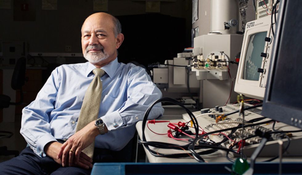 Many Hats: Although busy writing books and managing university programs, Baliga still oversees students in his lab.Photo: D.L. Anderson
His colleagues shared Baliga’s idea with GE’s new chairman and CEO, Jack F. Welch Jr., whose draconian management style had earned him the nickname Neutron Jack. “If he visited a plant and he was not happy, the building was left and all the people were gone—like a neutron bomb,” explains Baliga.
Thomas Jahns, a researcher who worked with Baliga at GE and is now a professor of engineering at the University of Wisconsin–Madison, confirms what it was like under Welch. “It was an intense time. [The researchers] were called on the carpet to come up with solutions: Either you deliver or you get out.”
In early 1981, Welch traveled to GE’s research center to be briefed about the new transistor concept—a high-pressure presentation for Baliga if ever there was one. “A lot of careers were on the line—mine in particular,” he says. But all went well, and within a year, Baliga and his colleagues were fabricating wafers with the new design. Initially, he dubbed the device the “insulated-gate rectifier,” in an attempt to distinguish it from ordinary transistors. But he later changed the name to insulated-gate bipolar transistor to avoid confusing application engineers.
The new IGBT successfully avoided catastrophic “latch up”—the thyristor-like continuation of current flow after a transistor is turned off. But it still switched off too slowly to be used for variable-frequency motor drives, and known methods for upping the speed of a transistor would ruin a MOS device such as this one. “We can use it for 60 hertz. Maybe we can run a steam iron,” was the disappointed conclusion of his GE associates, recalls Baliga.
With thoughts of Welch’s neutron irradiation no doubt swirling in his mind, Baliga devised a clever way to speed up the IGBT: electron irradiation.
Such treatment had been used on bipolar power rectifiers, but it damaged MOS devices. Baliga figured out how to apply just enough heat to repair the damage to the MOS structure while keeping the speed boost.
“I could control the speed all the way from low frequencies to as high as I wanted,” says Baliga. Within a few months the new process was being used to make chips. “Now everybody went bananas with this—now they had fast devices. They could start running with it. It just took off.”
Among the places that IGBTs went airborne was Japan, where Fuji Electric, Hitachi, Mitsubishi Electric, and others took interest in Baliga’s work and eventually began manufacturing these devices, in stiff competition with GE. And GE’s investments at this time in making very-large-scale integrated circuits went badly. In 1988, Welch decided to sell off GE’s entire semiconductor business. That move in turn rendered Baliga’s research expertise useless to the company.
Baliga’s bosses said they’d find a place for him in upper management, he recalls. “But in my heart, I still felt like I was a scientist,” he says. The offers he was getting from other companies weren’t attractive, however, and academic activity in power devices was nonexistent in the United States, Baliga says. But that didn’t mean he couldn’t create his own research program. The question was, where?
Baliga had often visited North Carolina’s Research Triangle Park, where GE had a power-electronics group, and he knew that MCNC, the Microelectronics Center of North Carolina, housed a state-of-the-art CMOS-fabrication line. With access to that facility, he figured he could do good research at nearby North Carolina State University, which was eager to recruit him. “He could have gone almost anywhere,” says Nino Masnari, who then headed the department, which was building up its semiconductor research program on a newly opened satellite campus.
So in August of 1988, Baliga moved to NC State, where he has taught and done research for a quarter of a century now. It’s also where President Obama visited just a few months ago to announce the creation of the Next Generation Power Electronics Innovation Institute—and a corresponding US $140 million grant to the university, which Baliga’s team at the university’s Future Renewable Electric Energy Delivery and Management Systems Center helped to win.
One goal of the new federally sponsored institute is to speed the development of MOSFETs and other power devices made with what are called wide-bandgap semiconductors, which outperform those made of silicon. One day wide-bandgap MOSFETs should be cheap and reliable enough to replace IGBTs. “If all goes well, my baby, which is now a big gorilla, will go away,” jokes Baliga.
But that’s fine with him. Despite his status as the father of the silicon IGBT, a narrow-bandgap device, Baliga has long championed its wide-bandgap rivals. Indeed, even while he was developing the IGBT at GE, he was also creating the first wide-bandgap power semiconductor, a gallium arsenide rectifier. About that same time, he devised a way to calculate from basic theory what semiconductor types function best for power devices—an expression now known as Baliga’s figure of merit—which highlighted the promise of silicon carbide and other wide-bandgap semiconductors. The trick is learning how to make these exotic devices cheaply enough to compete with silicon, a quest that Baliga and his students, along with many other researchers, are actively pursuing.
Baliga has also been deeply involved in the start-up scene. Companies he launched in the 2000s have created power semiconductors for cellular base stations and for managing the huge currents fed to modern microprocessors, to give just two examples. While all were commercially successful, none of these ventures has made him rich. “But that’s okay,” he says. “I get very excited just that people are using my chips.”
Indeed, without being at all aware of his role, millions of people around the world are benefitting from the power semiconductors Baliga pioneered. And with the demand for ever-more-efficient devices only going up, they will no doubt continue to do so for many years to come.
This article originally appeared in print as “The Power Broker.”