
In 1945, mathematician John von Neumann wrote down a very simple recipe for a computer. It would contain two key components: a central processing unit to perform calculations and logical operations, and a memory bank to store instructions and data.
Our computers and microprocessor-equipped gadgets still follow this basic recipe. But under the hood, of course, they are far more complex. No existing form of memory is good at everything. So to move instructions and data as fast as possible, engineers have had to compromise. Today’s computers use a smorgasbord of different memory technologies, exploiting the best parts of each.
This hodgepodge has worked quite well for decades, but it’s far from ideal. One of the biggest energy drains comes from shuttling data around the CPU and all the levels of memory that surround it. What’s more, our fastest memories lose their data if power isn’t continuously supplied to them. And the memories that are most compact—those that can store large numbers of bits in a small area—are slow, which is the main reason it takes so long for our gadgets and computers to wake up from sleep.
Making Magnetic Bits
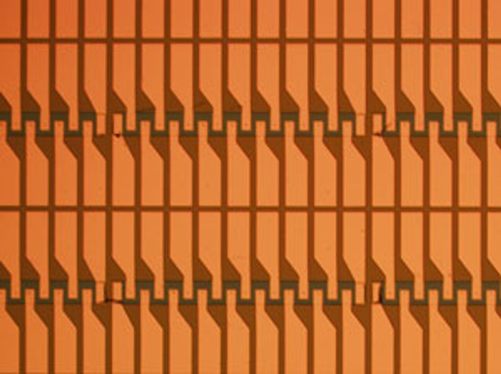
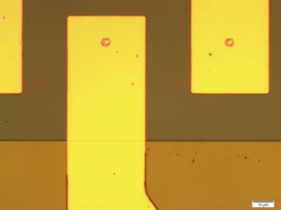
 A portion of a 1-kilobit array of magnetoelectric RAM (MeRAM) as viewed from above (top). The top electrodes of the bits are made from tantalum and gold (middle). The small circular dot on each electrode denotes the place where the electrode makes contact with the underlying magnetic tunnel junction, which contains the thin magnetic layer where information is stored. The magnetic tunnel junction (bottom) is shown from the side.Images, From Top: UCLA/Inston (2); UCLA
Those of us who work on alternative memories have long sought a way past these limitations. We’ve dreamed of creating a single, “universal” memory that could do everything well and could therefore replace the many kinds of memory we have now. It must be fast, to minimize the delays associated with reading and writing data, and it must consume little power every time it is used. We should be able to manufacture it on the same chip as a CPU, allowing us to put it close to the computational action, and be able to make it dense enough to compete with existing memories on cost. At the same time, we would like it to be nonvolatile—able to retain data without having to continuously draw power—so it can be shut down when it isn’t needed.
Such a memory is years away. But this vision has been enough to inspire a range of ideas for alternative memories that might one day fill the bill. Our team at the University of California, Los Angeles, has been working on what we believe is one of the most promising candidates: a form of magnetic memory called magnetoelectric random access memory (MeRAM). We have already created small arrays of this memory, and it has recently started to attract the interest of chip manufacturers.
In parallel, we and others have also been exploring how to use the same physical process that lets us write data to MeRAM to do something much more radical: Overhaul the von Neumann blueprint of the computer, by eliminating the long-standing distinction between logic and memory. With MeRAM technology, it’s possible to create logic that is its own form of memory—a switch that can both perform computations and remember. This switch would retain its state even when it’s powered down.
Such “nonvolatile logic” may one day spur a full overhaul of the microprocessor, allowing us to build chips that can very quickly shut off parts that aren’t being used in order to save energy, freeze their state if they lose power, and remember exactly what they were last doing the instant you turn them back on. In our lab we’re fond of calling this new form of instant-on electronics “Instantonics,” and we think it could dramatically enhance the speed and battery life of computers, tablets, and smartphones. It could also provide a massive boost to some of the most memory-intensive computing tasks, such as video and multimedia signal processing, pattern recognition, virtual reality, and machine learning.
The hierarchy of memory in a computer starts with static RAM, which is the fastest and is usually found on a microprocessor chip next to a computing core. Next, often on a separate chip or chips, is dynamic RAM, which is somewhat slower than SRAM, but also considerably cheaper. Like
transistor-based logic, both of these memories require power to retain their data. In fact, DRAM bits need to be continuously refreshed, or rewritten, to prevent them from losing data. Because of this limitation, long-term storage in computers is accomplished by two memories that do not need power to retain information: the traditional magnetic hard drive and NAND flash.
These nonvolatile data storage devices have their own drawbacks. Flash, which stores information as charge that is added to or removed from a transistor structure, can be made at high density and thus low cost. But the process of writing information to each bit is very slow—easily slower by a factor of hundreds than it is in DRAM. It also requires large voltages and can be done only perhaps 100,000 times. Hard disk drives, which store data in the form of the magnetic orientation of different patches, or domains, on a ferromagnetic disk, have better endurance. But they are even slower than flash because they rely on mechanically moving parts to read and write bits.
These shortcomings have led memory researchers to consider alternative, nonvolatile memories that use spin. Spin is a basic quantum-mechanical property of subatomic particles, such as electrons. In magnetic materials such as iron, cobalt, and nickel, it is the spins of the electrons that give those metals their overall magnetic properties—that is, their north and south poles. A particle’s spin is closely related to intrinsic angular momentum, which is the property that causes the particle to interact in particular ways with magnetic fields. But despite its name, spin does not have anything to do with actual physical rotation. Yes, the concept of spin is pretty abstruse, but for our purposes here you really need to know just two things. One is that spin has a direction; in other words, if a particle has spin, then that spin points somewhere. The other important concept is that in a material that has been magnetized, most of the individual electrons have spins that point in the same direction. That is what gives the material its magnetization.
Ordinary hard disk drives are, in fact, a form of spin-based memory. On the disk, each bit of data is stored as a microscopic patch of magnetic material, where all of the electrons have the same spin direction. To select a bit to read or write, the disk physically rotates underneath a read/write head, which also moves. To change a bit from a 1 to a 0, the head reverses the polarity of the magnetic material in the tiny patch, so that the spins in it point in the opposite direction.
The term “spintronic memory” refers to a specific kind of memory, also called magnetic RAM, of which there are several variants. These memories have no moving parts. The basic memory element in MRAM is a magnetic tunnel junction, a nanoscale sandwich of two magnetic layers separated by a thin insulating dielectric barrier. (In practice, several other layers are added to boost performance and provide contacts to the outside world.)
In the junction, one of the magnetic layers is pinned, which means the direction of its magnetization is fixed to serve as a reference. The other magnetic layer, which is referred to as the free layer, is where information is stored. The free layer’s magnetization can be switched so that it’s either oriented in the same direction as the pinned layer or 180 degrees in the other direction. The orientation of this free layer affects how readily current can quantum mechanically “tunnel” across the device, through the insulating barrier. So the value of the resistance of the device indicates the orientation of the free-layer magnetization, and thus whether the bit is 0 or 1.
Overall, the space needed for the wiring and other components makes spintronic memories less dense than hard disk drives. But they’re also much faster, less energy hungry, and more reliable because there is no mechanical motion involved.
The process that’s used to write to the memory bit, by altering the orientation of the free layer, turns out to be where most MRAM technologies have diverged. One of the earliest MRAM variants, which emerged commercially about 10 years ago, used the magnetic field generated by a nearby current-carrying wire to write data. This type of MRAM was the first to go into commercial production, and it can deliver fairly fast writing speeds on the order of a few tens of nanoseconds, hundreds of times as fast as flash and on par with DRAM. The drawback is that large currents need to be driven through the conducting wires to generate the magnetic fields needed for switching. This requirement prevents the memory cells from being scaled down to the small dimensions you need for modern chips, as it becomes harder and harder to drive sufficient currents through smaller wires and, as cells get closer and closer together, to ensure that magnetic fields affect only the target bit.
A second variant of MRAM, which is being pursued by many of the biggest memory manufacturers and chipmakers, uses a different physical phenomenon, called spin transfer torque (STT), to write information. In STT-MRAM, information is written to the magnetic bit by driving current directly through the device, as opposed to using the magnetic field created by a nearby wire. If the current running through an STT-MRAM bit is large enough, the electrons in it can be used to tug on the spins in the free layer and wrench them into the desired direction—either parallel or antiparallel to the spins in the fixed, reference layer.
Storing the Information
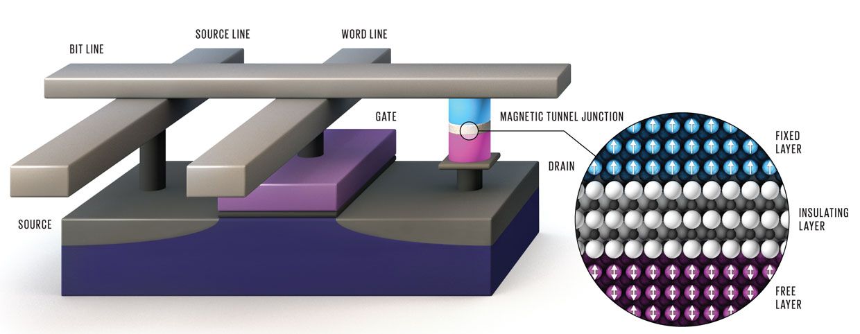
Both spin transfer torque MRAM (STT-MRAM) and magnetoelectric RAM (MeRAM) can use the same basic architecture to store data in the orientation of electron spin. Each bit in an array can be accessed at the intersection of two lines of electrodes—a source line and a bit line. A third electrode—the word line—is used to control voltage supplied to the bit. A single bit of information can be stored in the free layer of each magnetic tunnel junction. In STT-MRAM, current flows directly through the junction in order to write the bit. MeRAM, which boasts a thicker insulating layer, does not permit current to flow as readily and instead uses voltage-associated effects to change the state of the bit. In each case, the magnetization of the free layer can be flipped [inset, right]. When the magnetization of the free layer and that of the fixed layer (which serves as a reference) point in the same direction, resistance is relatively low. It is higher when the two magnetizations point in opposite directions. Note that a MeRAM transistor is much smaller than an STT-MRAM transistor, since it does not have to provide as large a current. As a result MeRAM cells are smaller overall, and arrays of them can be made more dense.
Over the past few years, a number of research groups including our team at UCLA have been able to show that STT-MRAM can be written in just 100 picoseconds, and with as little as a couple of hundred femtojoules of energy. That’s better than the first form of MRAM and on par with SRAM, but it is still not enough to rival the logic switches at the heart of the CPU. A typical CMOS transistor nowadays expends only about 1 femtojoule of energy per switch. Moreover, STT-MRAM does not allow much room for improvement in energy efficiency. The reason is a fundamental one: The device is essentially a wire. As current is driven through it, energy is lost to heat. And as with a wire, the narrower the device gets, the higher its resistance. Also, each memory cell in STT-MRAM needs a transistor to drive the write current through the device. Because the transistor needs to provide relatively large currents, it can’t easily be shrunk. So although STT-MRAM is picking up steam, its memory cells will have to stay fairly large—perhaps three to five times the size of DRAM cells.
It turns out, though, that many of the limitations of MRAM and STT-MRAM can be avoided by designing a device that uses voltage instead of current to switch magnetization. This approach to writing information is being actively pursued by several teams, including ours. It promises switching energies of about a femtojoule or even lower—less than 1 percent of what’s required with STT-MRAM.
Using an applied voltage is standard practice in semiconductors; that’s how modern MOS transistors work. It’s a voltage, after all, that opens or shuts the gate to the flow of charge carriers in the semiconducting channel beneath it.
Even so, it wasn’t immediately obvious that you could use a similar, voltage-based approach to manipulate spins. In order to store information, spintronic devices need materials that have a permanent magnetization, or magnetic moment. The best candidates are usually metals such as iron and cobalt. Unfortunately, conductive materials like these are also pretty good at blocking electric fields, preventing them from penetrating deep into the metal. The reason is that the natural motion of the electrons in such conductive materials easily scrambles electric fields that enter the material, “screening” the effects of an applied voltage much as a fast-moving river might overwhelm the flow of an incoming stream.
As a result, some of the earliest efforts to use voltage in spintronics aimed to make the devices with as little metal as possible. One way to do this is to take a semiconducting material like silicon or germanium and scatter magnetic atoms through it, creating what’s called a dilute ferromagnetic semiconductor. If a voltage is applied to this material, the resulting electric field won’t be screened as readily as it would in a metal. Instead, the field will pull or push on charges in the vicinity of the voltage gate, which in turn changes the magnetic properties of the bit.
The difficulty with this approach is that it is hard to get ferromagnetic semiconductors to work at room temperature, because their magnetic properties are too weak for their spins to withstand thermal fluctuations without losing alignment.
Fortunately, there’s another option. About 10 years ago, theorists began exploring what would happen if you tried to use a metallic magnetic material to make a very thin electric-field-controlled structure—about a nanometer, or less than 10 atoms, thick. This thickness is still greater than the distance an electric field can penetrate into a metal before being largely scrambled. But it’s thin enough that small changes at the surface of the material can have a big impact on the film’s overall properties, including the natural inclination of the spins to align in a particular direction. This idea was met with great interest and motivated researchers at Osaka and Tohoku universities, in Japan; at Johns Hopkins University; in our group at UCLA; and elsewhere to make memory devices based on this scheme.
The magnetoelectric RAM, or MeRAM, device we’ve been working on is one of these thin-film spintronic memories. In many ways it’s similar to STT-MRAM. For one thing, it can be made with the same cobalt-iron alloys. The main change is in the device structure and engineering of its interfaces. The layer that acts as the bit is very thin. And the insulating layer that in STT-MRAM would pass a current is made thicker, so that very little current can flow. This change in structure essentially turns the magnetic tunnel junction into a capacitive—instead of a resistive—device. When a voltage is applied across this capacitor, the resulting electric field alters the magnetic properties of the device’s free layer. This will change how strongly the bit’s spin is locked into an up or down orientation. The spin direction will begin to swing, and if the voltage pulse is cut off at the right time, the bit’s spin will end up pointing 180 degrees opposite its initial orientation. A small magnetic field or current can also be used to nudge the spin into the desired final state.
The benefits of this arrangement are impressive. Because MeRAM does not require a large current to switch, its transistor can be made much smaller than in STT-MRAM, resulting in much denser arrays. And we have already demonstrated that data can be written in less than a nanosecond, using just a tenth of the energy needed to write to STT-MRAM. As the devices get smaller and materials improve, we expect to be able to further cut down on the energy by as much as a factor of 100.
Last year, our team built a 1-kilobit array of this memory. That’s a small step compared with conventional memories, which now extend into the gigabits or even terabits. But this array demonstration, made possible in part with the support of the U.S. National Science Foundation, is an important proof of concept, and we’re starting to see some indication of commercial interest. Makers of semiconductor fabrication equipment, including Applied Materials, Canon Anelva, and Singulus Technologies, are working on special sputter-deposition and etching machines that can lay down and pattern the nanometer-thick layers of magnetic compounds needed to make high-density arrays of these devices.
The next step is to show that these memory arrays can be integrated onto existing CMOS chips. This integration will be done at relatively low temperature at the back end of the chip manufacturing process, when layers of metal wiring are used to connect the components of the chip to one another and to the outside world. This basic “back end of line” approach is already used to make MRAM and STT-MRAM and could be adapted to MeRAM as well. (There is, incidentally, a very different memory, resistive RAM, which also exploits these metal layers; it’s likely to be more useful for cheap, higher-density storage.)
If MeRAM can be integrated in conventional processors, it could potentially supplant all but the fastest SRAM on a chip. And because it should be easy to make compact, this memory will fit in the metal layers, where plenty of room is available. Thus this technique could bring memory functions that are now done off-chip in DRAM onto the processor. Memory cells would then be separated from the CPU by millimeters or even micrometers instead of centimeters, drastically cutting down on delay and heat-dissipation problems.
We can also apply the same voltage-switching approach used in MeRAM to do something even more radical: Make logic that is nonvolatile and so acts as its own form of memory. This idea got a boost in 2010, when our team received support from the U.S. Defense Advanced Research Projects Agency (DARPA) to investigate the possibility.
The spintronic logic devices we’ve designed take advantage of the way spins in a material tend to interact with one another so that they all line up in the same direction. Knocking one or more of these spins out of kilter with an electric or magnetic field will cause a wave of spin disturbances—or “spin wave”—to move through the material, like ripples moving out from a splash in a pond.
Riding the Waves
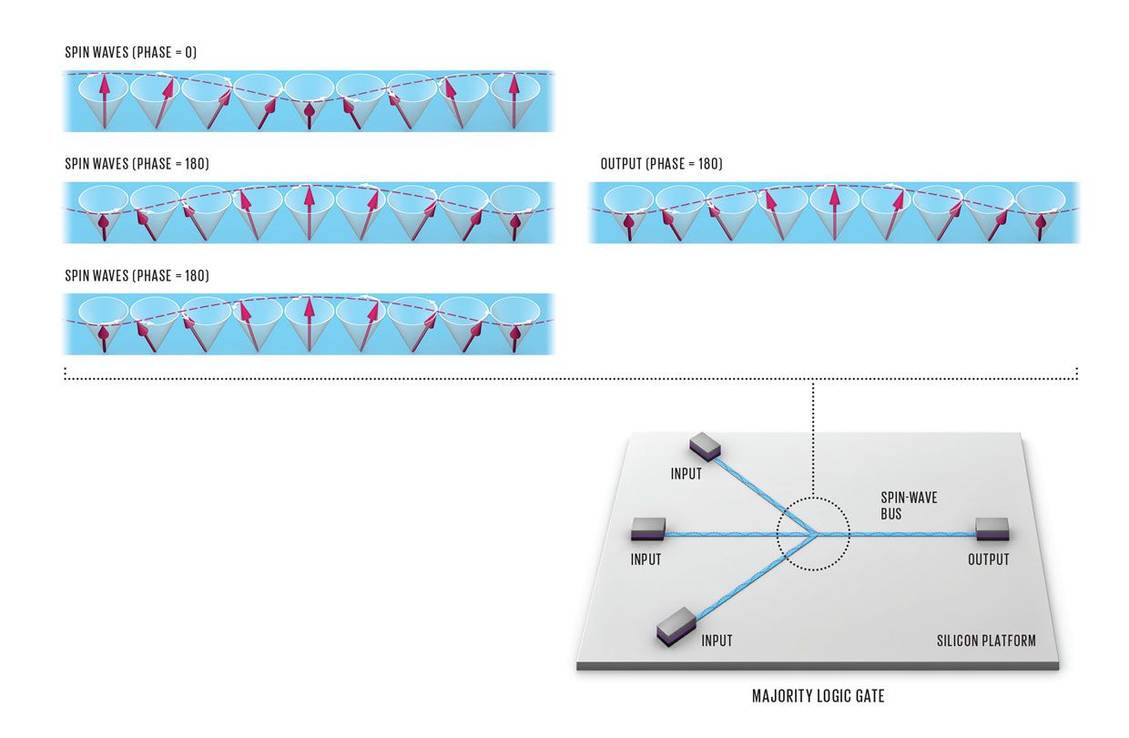
A voltage pulse can be used to knock an electron’s spin out of alignment, causing it to precess. This effect can be used to transmit information along a strip of magnetic material. The first perturbed spin will affect its neighbor and cause a wave of precessing spins to propagate down the line of electrons [top]. These waves can be made to take on two different phases, separated by 180 degrees, to represent a binary 0 and 1. Two waves with opposite phases can be made to interfere with one another, canceling out the spin perturbation. Logic gates, such as the majority gate, can take advantage of this interaction. The majority gate “votes” for whatever state constitutes the majority of inputs. This can be accomplished as shown [right], by causing three lines of spin-wave inputs to meet and interact. It can also be implemented along a single line, by introducing the voltage pulses that trigger spin-wave perturbations at three different points. In either case, MeRAM memory cells can be built on top of the logic gate to retain input data, trigger spin waves, and read out the result.
These disturbances can be created using voltages like those used to control MeRAM. But in this case, the voltage pulses are weaker, perturbing the spins instead of reorienting them by 180 degrees. Our experimental logic devices exploit these waves. In these devices, 0 and 1 do not take the form of the presence or absence of current. Instead they are represented by two different phases of a spin wave—a peak at a given position and time would be a 0, for example, and a valley would be a 1 (or vice versa).
To give you a sense of how spin waves can be used to perform calculations, we can take the example of the majority gate. A majority gate works by taking on the value of the majority of its inputs; typically there are three of them. Including the output, such a gate has four terminals.
In the device, the three voltage-controlled input terminals are used to create spin waves with a phase of either 0 or 180 degrees. The device is designed so that these waves meet and either interfere with or reinforce one another. At the output terminal, the detected signal will be the sum of the spin waves from the different inputs. If all three waves have the same phase, the output will share that phase. If there are two waves with opposite phases, they will cancel each other out, and the phase of the remaining spin wave will determine the phase of the output. Thus two out of three will win. In order to add nonvolatility to this logic operation, MeRAM magnetic memory bits can be integrated on each input and output terminal; they can be used to both input and store data.
Together with our collaborators at the University of California, Riverside, and the University of Massachusetts Amherst, we have simulated these majority gate devices and found that it’s possible to use them to create general-purpose computers with just one additional type of logic gate: an inverter.
Spin-wave logic’s ability to exploit phase doesn’t really have a counterpart in conventional logic. But the simulations suggest that logic built with this technology could have speeds in the gigahertz range, more or less comparable to those of today’s chips. At the same time, the spin logic would consume much less energy per operation, on the order of a hundredth of the amount consumed by CMOS.
Other approaches to nonvolatile logic are also being explored. One, which was also supported by the DARPA nonvolatile logic program, transmits information through magnetic perturbations between closely set, discrete nanomagnets. Others are investigating the movement of the walls between magnetic patches. In both of these approaches, it’s looking like the most energy-efficient operation may come from using an applied voltage.
Should one of these approaches succeed, we could start thinking about doing dramatic things to the microprocessor. We could overhaul the traditional von Neumann architecture and create circuits that don’t need a separate memory to perform calculations and don’t have to shuttle data to some external chip to make sure it’s not lost.
The implications would go well beyond improving the battery life of our personal gadgets. Chips that can run at extraordinarily low power could be very useful in devices that are physically difficult to access and therefore can’t be easily recharged. Examples include medical implant chips and sensors in hard-to-reach places, such as at high elevations, in space, below ground, underwater, or in environments otherwise dangerous to humans. With vast amounts of low-power, on-chip memory, these devices could also be substantially better at particular memory-intensive computing tasks, such as pattern recognition and machine learning. Defense and space applications will benefit from instant-on systems, which will mean power failure, radiation, and other disruptions will be far less likely to result in a loss of critical information.
There are even more exotic circuits still on the horizon. Topological insulators, materials that transmit current only along their surfaces, could potentially be used to make memories that switch with just a thousandth the energy needed by metal-based spintronic devices. But researchers are still exploring the fundamental properties of these materials. In the meantime, these recent spintronic results make it clear that there are things we can do now to greatly improve computing.
Taking full advantage of these technologies will require a willingness to move beyond the strange and somewhat inelegant mix of logic and memory we’ve relied on for decades. But once we get over the shock of pushing aside the status quo, we will find we can accomplish great things.
About the Author
Pedram Khalili is an adjunct assistant professor at UCLA, where co-author Kang L. Wang is a distinguished professor and the Raytheon Chair in Electrical Engineering. Khalili’s earlier focus was on fairly large microwave magnetic devices for RF applications. Moving to atomic scales was a bit of an adjustment, he says. Now he’s excited to see what big things these tiny devices can accomplish.