
Say good-bye to the node.
For 39 years, the node endured as the elusive and yet universally accepted metric that semiconductor specialists used to indicate how small their transistors were. Like depth readings on a wild descent into the infinitesimal, node figures were plotted out for the near future in a “road map” released annually by the semiconductor industry associations of Europe, Japan, Korea, Taiwan, and the United States. That map was, and is, a collection of the global semiconductor industry’s best ideas about how it was going to fulfill the Moore’s Law prophecy of a 30 percent shrink in transistor size—and consequent doubling in density—on chips every two years.
But now, in the first tremor of what promises to be a tectonic shift in the semiconductor industry, the node is no more. For decades, makers of logic chips used the concept of the “node” not only to measure their transistors but also to indicate how advanced their chip-fabrication lines were. Memory chipmakers, meanwhile, used a different measure, halfâ¿¿pitch, for the same purpose. Now lithography, the printing process at the heart of chipmaking, is being pushed to extremes to get to the end of that road map. These extremes will affect different devices on different timescales, but the end of the road looks the same for every device.
We’re pulling out all the stops for the current generation of chips. And if that sounds like a platitude you’ve heard before, consider this fact: Nothing significant that we’re using now will work to create the chips we plan to produce commercially just five or six years from now—least of all the current method of lithography. The next generation of chips won’t be possible without the next generation of lithography. And that, in turn, means that the next generation of lithography will depend critically on what happens to the different chipmakers. For example, memory technology, an industry that sees prices falling at the staggering rate of about 40 to 50 percent per year, faces significant pressure to scale up faster than logic devices do.
Industry observers will not be surprised by the death of the node, as the node and half-pitch, once synonymous, have been diverging for some time. This minor change foreshadows a big change in the way the lithography business will deal with memory versus logic. For the first time, lithography will apparently have to adjust to follow both microprocessors and the different memories—including NAND flash, DRAM, and SRAM—down their respective paths, which have been diverging for decades.
Optical lithography, the most important and technologically demanding aspect of chipmaking, is a pillar that won’t be easily toppled. But the technology is at a critical point. The technique, which uses radiation with about half the wavelength of purple light, is fast approaching steep, if not insurmountable, obstacles. Unfortunately, none of the various technologies proposed over the years to replace it has inspired confidence that it will be ready when the time comes.
Nevertheless, one thing is clear. From now on, the relationship between chips and lithography will be two-way. Not only will the fate of chips depend on the future of lithography, but also the reverse will be true.
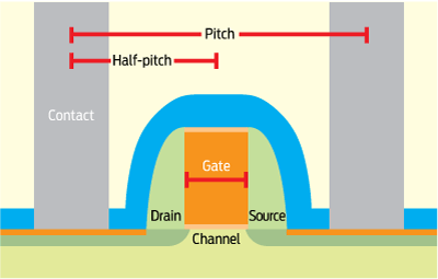
Let’s start by defining our terms. Today’s most advanced microprocessors use a 32-nanometer process, and thus are said to be at the 32-nm node. To get a sense of how infinitesimal 32 nm is, consider that to span the width of the lowercase letter l on this page, you would need to bunch together more than 9500 32-nm objects. Node in this context has historically been used to refer to the size of the smallest parts of the transistors on the chips. Until the late 1990s, that was typically a feature called a gate. But there is a very fuzzy relationship between the technology node’s number and the actual dimensions of the gate it purports to signify. In fact, the International Technology Roadmap for Semiconductors, the industry’s guide star, abandoned the term in 2005, but its usage has persisted.
In both logic and memory chips, each of the vast profusion of transistors acts like a switch that allows electrons to flow through the device. A metal-oxide semiconductor field-effect transistor (MOSFET), the kind found on virtually all chips, has three main parts: a source, a drain, and a gate. A voltage applied to that gate lets the electrons flow from source to drain. Physically, the gate sits between the source and the drain.
On a chip, that translates to the distance between the parallel metal lines, called interconnects, that carry the electrons through the chip. These interconnects are stacked today in multiple levels, and as many as 10 can populate a chip (a cutting-edge chip could have 10 kilometers of interconnects). The distance between these metal lines at the first level is called the pitch, and logically, the half-pitch is half that distance.
The half-pitch of the metal lines on the first and densest level is special, because that distance was what once defined not only the half-pitch but also the gate and, consequently, the node. But by 2000, it was a dicey relationship. The half-pitch was becoming bigger than the node.
So, for example, in 2005 the gate width on an Intel micro-processor was 32 nm. The node was called “65 nm,” but the half-pitch for the first level of wires was 105 nm. Confused yet?
The node’s dilemma
The half-pitch of the first wiring layer is the defining feature for memory chips, while the gate length is the gauge for logic manufacturers. Neither is entirely representative of the node.
The trouble with the terminology started in the early 1990s, when these gate widths fell down a steep slope [see table, "Pitch Counts”]. For logic devices, the gate length became the smallest feature, but for memory the half-pitch remained the smallest feature. Those were simpler, happier times. The industry sold microprocessors based on how fast the chips could process instructions, and that rate was pretty much directly related to how small the gate width was. We in the industry (I was working for Advanced Micro Devices, in Sunnyvale, Calif., at the time) called it the time of the megahertz wars. These wars drove the shrinking, with the result that the gate width got much smaller than the half-pitch.
So it was that, in the second half of the 1990s, the market’s endless appetite for better-performing logic devices drove microprocessors—which used to lag two to three years behind memory in half-pitch—to start closing the gap. Because microprocessor speed was largely determined by the dimensions of the gate, by 2000 the gate had become the smallest feature produced in the semiconductor industry.
While speed is also a key parameter for memories, there was no similar war between memory manufacturers seeking to drive up the frequency with which transistors execute their instructions, known as clock frequencies. Memory makers focused on reducing the size of each memory cell on their chips so that they could squeeze ever more bits into less and less real estate.
So let’s recap. Today’s cutting-edge 32-nm-node logic chips are actually at a 50- or 56-nm half-pitch . Today’s cutting-edge memory chips, if they were described in logic terms, would be at the 22â¿¿nm node , but they are in fact at about a 34-nm half-pitch, putting them ahead of logic development by a full chip generation.
The unifying factor is that both memory and logic have always been made with optical lithography. But because memories and logic have different shrink rates, memory makers will have to be the first to make the transition from optical lithography to the lithography technology that will succeed it, called extreme ultraviolet lithography (EUV). People who dread the transition to EUV often claim that it’s not optical lithography, putting it in the same zoo with the other next-generation lithographies, such as electron beam lithography and imprint lithography. I prefer not to distinguish between optical and EUV: EUV is optical, inasmuch as it is electromagnetic radiation, only with a wavelength that’s about one-fifteenth as long.
The death of optical lithography, chipmakers have been known to say, is always seven years away. That joke was new 30 years ago, when chips were being fabricated at the 10-micrometer node. Today’s chips squeeze 4 billion transistors into a space smaller than a postage stamp. The technology that brought about that stunning advancement, and the key driver of the semiconductor industry (which this year is expected to have revenues of US $200 billion), is this method of tiny writing called lithography.
Lithography is why Moore’s Law endures after 44 years. Nevertheless, for the last 20 years, experts have been uneasy about lithography, which projects the fabulously complex patterns of a modern chip onto a semiconductor wafer using electromagnetic radiation with wavelengths shorter than those of visible light.
Fundamentally, optical lithography hasn’t changed much in almost 50 years. It has become more sophisticated, but its kinship to old-time film-and-chemistry photography is still discernible. Microchips start out as small blank patches on a silicon wafer about the size of a dinner plate. The virgin wafer is shuttled through a series of machines in a chip-manufacturing plant the size of a couple of American football fields. At the end of its journey through hundreds of tools, the wafer emerges inscribed with the patterns of hundreds of identical microchips. The wafer is then broken up into these constituent microchips, which are sent out into the world to populate laptops, thumb drives, cellphones, and the GPS in your car. The patterns that distinguish all these different kinds of chips are created with optical lithography.
First, the wafer is covered with a thin insulating layer and then with a light-sensitive material called photoresist. Light streams onto the resist through an opaque mask with holes that let light through to form a pattern. This system projects postage-stamp-size patterns onto the wafer until the entire wafer is covered with identical microchip patterns. The exposed areas of the photoresist are weakened when the light hits them, and then a corrosive plasma etches the pattern into the silicon. The leftover photoresist is washed away, leaving the photoresist pattern engraved into the semiconductor wafer.
The process has gotten more complicated with each generation of shrinking features. Lithography toolmakers have had to reduce the wavelengths of light they use to project chip patterns through the masks. They’ve also had to find heroic optical tricks to finesse the light into depositing patterns far smaller than the wavelengths themselves.
The shorter the wavelength, the finer the resolution of the features you can print on the chips and the more transistors you can squeeze onto the chip. The history of semiconductor lithography is essentially the history of the search for stronger and shorter-wavelength sources of light. The first commercial lithography tools were manufactured in the early 1980s. They started skirting the edge of the visible spectrum with light at a wavelength of 436 nm, somewhere between violet and indigo. In 1987, steppers graduated to the ultraviolet 365 nm of mercury lamps and then to 248 nm in 1993. Finally, in 2001 the industry arrived at the 193-nm light, derived from an argon-fluoride laser. This laser, still used today to create patterns with feature sizes down to 38 nm, is projected through massive lenses that weigh nearly half a metric ton and cost several million dollars.
When semiconductor lithography began in the 1960s, the feature sizes of transistors were much larger than the wavelength of the exposure light. To print his original transistors, Gordon Moore actually cut patterns into Rubylith and projected them onto chrome-covered glass plates, or masks, using 16-mm movie-camera lenses that Robert Noyce had bought in a northern California camera shop for a few hundred dollars. Moore’s transistors had a minimum feature size of around 100 µm, big enough to see with the naked eye.
Lithography had to keep up with feature sizes as they shrank to the size of the wavelengths of light itself—in the hundreds of nanometers—and then, more recently, vanished into mere fractions of the exposure wavelength.
As each image is exposed onto the semiconductor wafer, the lenses reduce the images 75 percent. Such sophisticated systems can expose more than 140 wafers per hour. Advances of this sort have improved resolution by a factor of about a thousand from the days of Moore and Noyce and the movie-camera lenses.
Impressive though it is to be printing today’s 38-nm features with 193-nm light, what the industry would like more than anything else is to get back to printing features that aren’t any smaller than the wavelength being used to print them. Here’s why. Light diffracts when it shines through the mask, spreading out and blurring the edges. However, you want to capture as much of the light as possible to produce a good image. That means you need some pretty good tricks to corral all the light into the pattern. If you can’t, your image will be blurry.
Because of tricks like water-immersion lithography—which increases resolution by replacing the standard air gap between the lens and the wafer surface with a liquid—chipmakers have been able to print sharp images within these parameters. But that ability has come at a great cost. ASML, Nikon, and Canon have all pushed water-immersion lenses as far as they can. Efforts to switch from a wavelength of 193 nm to 157 nm have failed because of difficulties with optical materials.
Most industry experts agree that features of complementary metal-oxide-semiconductor (CMOS) silicon transistors will continue scaling to below 20 nm. But that won’t happen without extreme ultraviolet lithography.
Extreme ultraviolet lithography uses a wavelength of 13.5 nm, right near the point where the deep ultraviolet becomes X-rays. If we could harness light at that wavelength, we could continue shrinking features without many of the resolution enhancement tricks we have developed to push 193-nm lithography to the limit. ASML Holding, where I am chief scientist, recently introduced an EUV lithography system that can produce chips with features smaller than 30 nm. Nikon reportedly has a similar tool in development.
ASML expects to ship its first commercial EUV production lithography systems next year. We have already installed two EUV development tools—one at the Albany NanoTech Complex, in New York state, and the other at IMEC, in Leuven, Belgium. These machines produce patterns with a 28-nm half-pitch, better than the so-called 22-nm node.
These EUV developments are welcome, but they shouldn’t be interpreted as proof that EUV has arrived. The systems are experimental, capable of turning out chips at a rate of a few wafers per hour, much slower than would be needed for a commercial system. EUV still faces significant technical challenges. Consider the contortions we have to go through inside the box to get 13.5-nm radiation. It can’t be done with any traditional light source. Instead, we use a big carbon dioxide laser to vaporize liquid tin droplets [see illustration, "Seeing the Light"].
First we boil the tin, and then we drip the liquid tin in carefully timed droplets, synchronized to the firing of the CO2 laser so that it hits each tin drop as it falls. When the laser hits the droplet, the tin is vaporized, and 13.5-nm photons are released. A spherical reflector mirror takes this radiation and channels it into the optical system. Quite a bit of the original radiation is lost in the process because you can capture only what is collected in the reflector, and the reflector does not surround the tin droplets completely. The upshot is that only a small percentage of the radiation created at the 13.5-nm wavelength reaches the photoresist to make the pattern.
And that’s just the first challenge. At 13.5 nm, your optics can’t be made of glass, because glass—and air, and just about everything else—absorbs 13.5-nm radiation. You need a good vacuum to prevent EUV light from being absorbed by stray molecules. You need to use mirrors rather than lenses, and that brings up the next issue: About 30 percent of the light that hits that mirror is absorbed. Finally, not all the radiation emitted by your CO2 laser and tin setup is 13.5â¿¿nm radiation—some of it is infrared and is lost as heat. EUV’s critics say that too much power is necessary to yield the number of photons required to expose wafers at the chip fab.
The mirrors in our EUV lithographic system are based on Bragg reflection, a concept used for optical fibers and other waveguides. To create a strong Bragg reflector, you start with a rigid substrate, then coat it with several dozen alternating layers of molybdenum and silicon. The layers must be spaced with a uniform thickness of about half the wavelength to reinforce the reflected wave as it bounces off the many dozen layers. With this staggering technique, it’s possible to make a surface that’s about 70 percent reflective (the other 30 percent is absorbed by the mirror surface).
The EUV development tools use a different light source. They still use the tin droplets, but instead of a CO2 laser, they vaporize the tin drops with an electrical discharge—a small lightning bolt, basically. These have proved rather inefficient.
One of the many technical challenges of making EUV work is figuring out how good the vacuum has to be to prevent EUV light from being absorbed by stray molecules.
Who are the potential customers for EUV? Anyone who wants to stay on the road map implied by Moore’s Law: big memory makers that have to shrink relentlessly, the largest microprocessor companies, and chip foundries.
But the majority of semiconductor companies don’t and won’t need to be at the cutting edge. Consider the chip-foundry business, which accounts for a large and growing share of the overall chip business worldwide.
Taiwan is home to several chip foundries, the two biggest being Taiwan Semiconductor Manufacturing Co. and United Microelectronics Corp., both headquartered in Hsinchu. A chip foundry fabricates anyone’s chips, on a contract basis. Unlike integrated device makers like Intel, Samsung, and Toshiba, which design and build all their own chips, some semiconductor companies do none of their own fabrication. Others have evolved from a past where they made their own chips to becoming “fab-lite,” where they retain some facilities to develop the initial technology but then send their volume business to foundries. This allows these companies to do rapid development under their own control and avoid the cost of massive fabs for volume. More and more companies in the United States and Europe are taking these approaches because they believe that building a new fab (which can cost about $5 billion) is an impossible expense in the current economic climate. In the United States alone, AMD, Freescale, and Texas Instruments all recently went fab-lite.
Soon only a few foundries, many of them in the Far East, will remain to run all these companies’ production lines. Others include Chartered Semiconductor in Singapore and Semiconductor Manufacturing International Corp. in Shanghai, as well as IBM Microelectronics in East Fishkill, N.Y., which makes processors for its own equipment but has also become a dominant foundry for game processors. AMD recently spun off its manufacturing operations to start Globalfoundries, a joint venture with the government of Abu Dhabi.
About half the foundry customers need chips that can be fabricated with the previous generation of process technology—currently 65 nm. Another 40 percent of foundry customers use even larger, earlier nodes. At most, only 10 percent have orders that require the most up-to-date chipmaking technology, to keep up with the likes of Intel and Samsung. These customers include companies that create graphics processors, FPGAs, and phone chips. Many foundry customers are focusing on design innovation, which may or may not require being at the forefront of chip-fab technology.
The standard sedative to EUV anxiety is the assurance that the gap will be bridged by double-patterning lithography, a technique of last resort that improves the resolution possible with 193-nm light by making two or more exposures, slightly shifted with respect to each other, and with two or more different masks [see “Seeing Double,” IEEE Spectrum, November 2008].
But double patterning is more cumbersome than many people realize. The trouble comes down to design restrictions, cost, and yield. To understand why, let’s go back to the foundry customer. With double patterning, these companies face a horde of new design restrictions. For example, with double patterning at 193-nm wavelengths, the only things that are easy to print are parallel or perpendicular lines and spaces. It’s quite difficult to print holes or elbows, and if you’ve ever looked at an actual (but unexceptional) circuit design, it’s absolutely lousy with zigs and zags.
So, first, companies painstakingly rework their designs to meet these onerous restrictions (no elbows! no zigs! no zags!). Then they’ve got to split the design into two or more parts. There is just no easy way to do that. Different electronic design automation companies are working on that problem, but none of them has been able to create the vaunted “black box” method, an ideal tool that will send the design on its way, no brain required.
Double patterning also demands more process steps, which again adds to the cost by cutting effective throughput, increasing fab cycle time, and adding additional defects. If your original process could yield 100 wafers an hour, using double patterning will leave you with much less. If you’d been turning a profit at 100 per hour, there’s no guarantee you will at 50.
Then there’s depreciation. Most fab owners keep their tools running 24 hours a day because they depreciate at the staggering rate of several thousand dollars per hour. That’s one of the major problems with double patterning. Cutting your throughput means you’re losing thousands of dollars an hour. Pretty soon you’re talking about real money.
Memory-chip manufacturing doesn’t require as many masks as logic does. Where memories have only a few wiring layers, state-of-the-art logic has a complicated stack of as many as 10 metal layers. Consequently, a set of masks needed to make a logic chip is going to cost more than a set for a memory chip. Both processes require the use of expensive masks. And masks need an inspection tool to insure against infinitesimal flaws. Yet another tool is needed to repair these flaws, another expense that neither logic nor memory manufacturers can avoid.
Memory makers don’t care as much about the cost of the masks because they don’t use as many. For them, a single mask set will make up to 100 million chips. A $1 million mask set, even doubled, works out to about a penny per chip. But for logic chipmakers, the economics are completely different, because the vast majority of mask designs may be used to make only a few hundred wafers. That’s because of the punishingly rapid evolution required to keep developing the latest features for cellphones or digital cameras.
If we meet our targets for EUV throughput, EUV is preferable to double patterning because it lets layers be exposed with single masks. Double patterning begins to fail at about 20 nm. Lens designers at Carl Zeiss (ASML’s supplier) believe we can build EUV optics capable of reaching at least an 11-nm half-pitch.
The principal logic makers are spending hundreds of millions of dollars on R&D every year to keep scaling their transistors, in speed as well as in physical size. Memory chipmakers, on the other hand, are now in glorious pursuit of the “Grand Unified Memory”—one technology that will do it all, easily taking over for the NAND flash memories you find in your MP3 player and USB drives, and the DRAM that dominates applications for high-speed (but power-hungry) computation. The contenders for this crown include phase-change memories, resistive RAM, and spin torque transfer magnetic RAM (STT-MRAM), but these find themselves approximately in the same place as EUV—each concept has been proved and even demonstrated, but it’s not quite ready for prime time.
Is it worth it? That’s the billion-dollar question. Scaling won’t continue forever, if only because we will eventually be down in the atomic realm.
Right now we’re at 34-nm features. Let’s assume no features can be smaller than the spacing between one atom and the next, which in silicon is 0.546 nm. Within a few years, progress won’t depend so much on making transistor parts smaller. Instead, it will increasingly depend on new transistor designs and on materials that will make the transistors and the chips they reside on unrecognizable. In the next few generations of shrink, the industry needs EUV lithography to continue Moore’s Law economics.
The enormous capital investments required by optical lithography and silicon manufacturing mean that no new technologies will easily displace these workhorses. To take over, any contender technology must build on, and incorporate, the incumbents.
About the Author
BILL ARNOLD has been chief scientist at ASML since 1998, which means he’s helping to shape the next generation of lithographic processes.