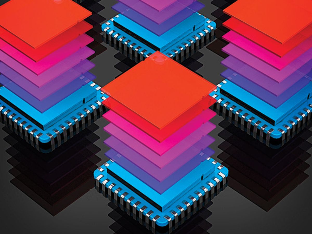
Chipmakers Push Memory Into the Third Dimension
Samsung, Micron, and SK Hynix bet that transistor redesigns and chip stacking will make memory smaller and faster

A 3-D revolution is slowly making its way across the chip industry. Intel set it off in 2011 when it debuted logic chips bearing transistors that pop out of the plane of the chip. This year, memory makers are joining the game with two innovations of their own.
If you upgrade your smartphone in 2014, chances are you won’t see either of these technologies inside it. They will appear first in high-performance (and high-margin) processors and solid-state drives. But analysts say it’s only a matter of time before these 3-D memories migrate to consumer gadgets. And that could mean big gains in speed and storage space.
One of the 3-D memory movements centers on NAND flash, a memory that’s nonvolatile—that is, it holds on to information even when it’s powered down. This flash memory is already used to store data in smartphones, tablets, and many laptops and is supplanting hard drives inside data centers.
Flash stores data in transistors, by injecting or draining electrons from a conductive patch called a floating gate. The value of a gate can be read because the electrons inside it alter the conductivity of an adjacent current-carrying channel.
But flash, which celebrated its 25th anniversary in 2012, is now showing its age. As chip features shrink, cells sit closer and closer to one another, increasing interference and the chance of corrupted data. What’s more, fewer electrons—mere dozens in today’s most advanced versions—can be fit inside any cell. As a result, cells are more liable to leak charge and be affected by tiny changes.
Memory designers reckon the solution lies in the third dimension. And the first company with a fix is top memory maker Samsung, which announced in August that it had already started production on a 128-gigabyte “vertical” NAND chip. SK Hynix, another South Korea-based firm, and Micron, based in Boise, Idaho, should ship 3-D NAND chips this year.
The companies are expected to turn each line of memory cells on its side, stringing them vertically in a forest of pillars. This will allow the memory manufacturers to take what’s essentially a right turn around Moore’s Law: They’ll pack more bits together not by shrinking features but by layering cells.
The change in architecture is expected to drive down the cost per bit and relax lithographic printing requirements. Indeed, Samsung’s new 3-D cells are likely made with a 30- to 40-nanometer process, a few generations behind the current, 20-nm class, says Dee Robinson, a senior analyst at IHS in El Segundo, Calif. With bigger cells and more electrons, Robinson says, “it’s actually a better performing chip.” She adds that it’s still unclear how quickly the cost of the new technology will decline to match that of traditional 2-D flash. But IHS estimates that 3-D flash will make up more than half of the NAND market by 2017.
The move carries some risk. “It involves technologies that have never been put into production before,” says analyst Jim Handy of Objective Analysis in Los Gatos, Calif. While some flash manufacturers are moving to 3-D, others, such as Intel, SanDisk, and Toshiba, are expected to stick with planar NAND for the moment, by taking advantage of new insulating materials. But they will inevitably be forced to switch to 3-D, Handy says.
A second 3-D technology—the Hybrid Memory Cube, or HMC—will also be ramping up in 2014. This effort focuses not on storage but on the computer’s memory workhorse: dynamic RAM.
The HMC won’t be any denser, smaller, or cheaper than an ordinary DRAM chip—it’ll be faster. It’s designed to surmount the “memory wall,” a communications bottleneck that has developed between multicore CPUs and memory, says Mike Black, a technology strategist at Micron. “The latest generations of high-performance CPUs are not capable of getting access to enough memory bandwidth,” Black says.
Micron developed the HMC in collaboration with SK Hynix and Samsung as well as more than 100 other semiconductor firms, research institutions, and potential customers. Their aim was to change the way systems handle DRAM signals. Instead of forcing DRAM chips to drive communications straight to a processor, the HMC off-loads most of that responsibility to a high-speed logic chip. DRAM dies are stacked atop this logic layer and are connected using thousands of copper wires called through-silicon vias (TSVs).
These vias allow the DRAM chip broad access to its bus; the logic layer cuts the number of connections that information must traverse on its way to the CPU. “This is the first commercial memory product offering [TSVs] as a standard part of the construction,” Black says.
Micron announced in September that it had begun shipping the first samples of its 2-GB memory cube. They’re expected to be produced at volume later this year, along with a 4-GB version. A single cube can offer 160 gigabytes per second of bandwidth, Micron says, compared with about 12 GB/s for current DRAM and 20 for the next generation, DDR4.
The HMC is quite fast, says Handy of Objective Analysis, but its success will hinge on finding a sufficiently large market to drive down costs. A large player such as Intel could sway the technology’s fate. But “so far,” he says, “Intel’s been playing it close to the vest.”
This article originally appeared in print as “Memory In the Third Dimension.”
