The Conversation (0)

Illustration: Harry Campbell
The transistor isn’t shrinking the way it used to. The best ones we have today are a patchwork of fixes and kludges: speed-boosting materials that push or pull on the silicon center, exotic insulators added to stanch leaks, and a new geometry that pops things out of the plane of the chip and into the third dimension. Now, to keep Moore’s Law going, chipmakers are eyeing another monumental change in transistor architecture.
This time, they’re taking aim at the current-carrying channels at the very heart of the device, replacing the silicon there with germanium and compound semiconductors known as III-Vs. If all goes well, these materials could usher in a new generation of speedier, less power-hungry transistors, allowing for denser, faster, cooler-running chips.
But for alternate transistor channels to be accepted, engineers must find a way to build them on industry-standard silicon wafers. That’s no small feat. The atoms in the alternative semiconductors are spaced farther apart than in silicon, making the crystals difficult to grow without creating device-killing defects.
Still, industry experts say, it is quite possible that silicon fabs will ramp up production of these transistors as early as 2017. One promising approach, under development in Belgium, saves on materials and minimizes defects by precisely depositing the new materials into nanometer-scale trenches etched into standard silicon wafers. The resulting chips could trim energy consumption at data centers, boost the battery life of mobile devices, and help keep Moore’s Law going well into the next decade.
Modern transistors are built into silicon wafers through the addition of trace amounts of other materials, called dopants. Dopant atoms alter the electronic properties of the material in order to form the three core parts of the transistor: the source and drain regions, which spit out and receive charge carriers, and the current-carrying channel, which runs between them.
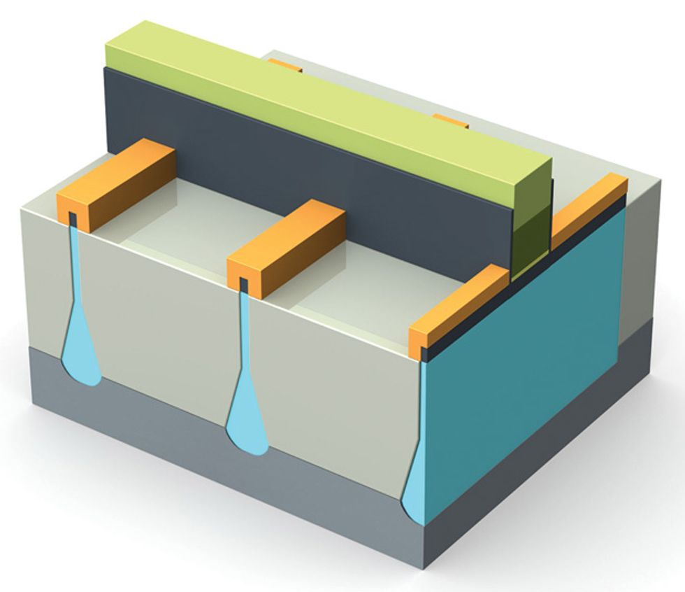
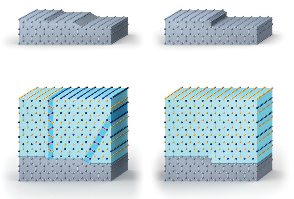
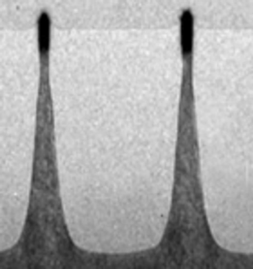 Up and down Trenches cut into silicon may be filled with germanium to make higher-speed, lower-power p-channel transistors. Researchers are moving toward building 3-D transistors with this alternate material. In the illustration above, germanium (blue) replaces traditional silicon in the current-carrying channel region. The channel is surrounded by insulating silicon dioxide (light gray) on top of silicon (dark gray). The micrograph (right) shows the cross-section of trenches for roughly 12-nm-wide channels.Illustration: Emily Cooper; Image: Imec logic program
For decades, chipmakers could speed up their microprocessors simply by shrinking the transistors and packing more of them onto a chip. They relied on a basic rule: Smaller transistors switch faster and consume less energy in the process. But in the late 1990s, this rule started to break down. As chips got more and more dense, power consumption began to put circuits at risk of overheating.
One way to tackle this heat problem is to lower the supply voltage—the voltage that is applied to the drain to pull charge carriers across the channel. This reduces power consumption, but it also means that less current is available to charge capacitors down the line, ultimately resulting in less speedy circuits.
Indeed, by the mid-2000s, CPU clock speeds began to stall. Companies began to work around the problem at the processor level by introducing multiple cores. But heat problems have persisted, and with each successive jump in transistor density, the fraction of transistors that may be active at any one time has gotten smaller.
At the same time, chipmakers have devised new ways to boost performance without adding more heat. One early strategy, debuted by Intel in 2002, was to mix silicon with germanium in the source and drain regions of the transistor. Atoms in this alloy are spaced differently than in pure silicon. The resulting strain alters the crystal properties—and thus the electrical properties—of the silicon channel, boosting the speed with which an electron or a hole (the absence of an electron that responds to an electric field as if it were a positive charge) could be tugged through the device. This hike in mobility resulted in faster-switching transistors that can carry more current for a given voltage, which makes for faster circuits, too.
Now chipmakers are adapting this basic strategy to make a more drastic change: the wholesale replacement of the silicon channel. A few materials have emerged as front-runners for the two kinds of transistors needed for logic circuits. For the positive-channel field-effect transistor (pFET), which carries holes across the channel, the leading candidate is germanium, which sits just below silicon on the periodic table and can transport charge four times as fast. For the negative-channel FET, or nFET, which depends on the movement of electrons, engineers are considering a mix of elements from groups III and V of the periodic table. One of the most promising is indium gallium arsenide (InGaAs), which boasts an electron mobility of about 10 000 square centimeters per volt second, more than six times that of silicon.
Intel, which has traditionally led the industry in transistor design changes, has already done some work on alternative transistor channel materials. In 2009, the company reported it had made InGaAs devices with a gate length of 80 nanometers. Although twice as long as what was then state of the art for plain silicon chips, they were shown to perform just as well with less power. The company has since incorporated the materials into new 3-D devices, called FinFETs, which have channels that pop out of the plane of the wafer.
But to build its InGaAs transistors, Intel had to blanket an entire silicon wafer with a fairly thick layer of the III-V material, then etch away the unneeded areas. That’s too expensive for high-volume production, says Richard Hill of the U.S.-based nonprofit Sematech, a chip industry research consortium.
The future, Hill says, lies in the alternative approach pioneered by Imec, a research outfit headquartered in Leuven, Belgium. There, a team of engineers, now 50 strong, has been working for more than 10 years on a way to grow each of the billions of transistor channels on a silicon chip in trenches just tens of nanometers across.
The approach is so attractive that last year Sematech abandoned its own wafer-blanketing approach to follow suit. And although Imec cannot disclose which industry heavyweights may want to use the approach, there are strong indications of interest. “[It’s] a very valuable option that we are taking into consideration,” says Lukas Czornomaz, a researcher in the Advanced Functional Materials Group at IBM Research–Zurich.
Imec’s work is based on a simple axiom of crystal growth: The right geometry can make all the difference. The Polish chemist Jan Czochralski discovered this in 1916 when he showed that it’s possible to make nearly perfect crystals by drawing a seed crystal from a bath of molten metal. A key lesson was that growing material in narrow columns limits defects. The most common defect occurs when an atom fails to adhere to the right spot, causing an entire plane of atoms to go missing down the line. Fortunately, these defects tend to propagate at an angle of around 45 degrees to the direction of growth, and if crystal growth starts with a long, narrow neck, the dislocation will generally propagate for just a short distance before reaching the edge, where it terminates.
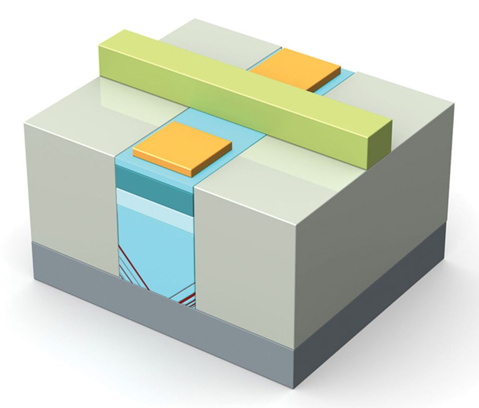
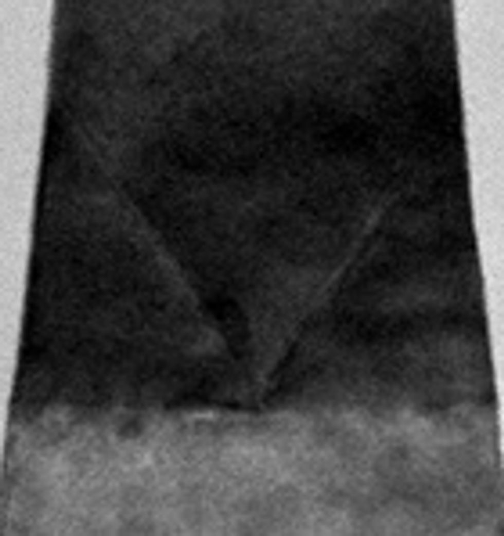 Where the defects stop Alternate channel materials for n-channel transistors are more difficult to work with; the research has not progressed as quickly toward a 3-D architecture. One approach for a planar transistor (above) is to grow indium gallium arsenide (darker blue) on other compound semiconductor layers. Defects in the crystals (diagonal lines) grow at an angle and terminate on the side of the deep trench instead of reaching the surface. This is also shown in the micrograph (right) of a silicon-germanium mix.Illustration: Emily Cooper; Image: Imec logic program
Growing each of the billions of nanometer-scale transistor channels in a tiny vat to make a chip would be impractical. But engineers can still take advantage of this geometric “necking” effect when growing crystals in vapor-filled reactors. The pioneer of this approach was Eugene Fitzgerald, a professor in the materials science and engineering department at MIT. In the 1990s, while based at Bell Laboratories, he showed that small patches of III-V material could be built on silicon if the “neck” that begins the crystal is built into the bottom of a rectangular trench that’s about twice as deep as it is wide. By the time the material is flush with the surrounding silicon surface, most of the defects have ended at one of the trench’s sidewalls [see illustration, "Where the Defects Stop"].
Matty Caymax, a chemist who specializes in postsilicon device fabrication at Imec, set out with his colleagues to see if they could make this approach fast, robust, and reliable enough to work in silicon fabs. Trenches themselves aren’t new to the semiconductor industry: For 15 years, fabs have etched away silicon and then refilled the trenches with silicon dioxide. Such “shallow trench isolation” creates stretches of insulating substrate between transistors so they can be packed closer together with minimal electrical interference.
Because silicon dioxide is noncrystalline, it can be packed into a trench without regard to where each individual atom ends up. Filling troughs with materials that have a high charge-carrier mobility is another matter. To work properly, they must form high-quality crystals, even though the spacing between their atoms is quite different from that of the silicon they are grown on. Germanium atoms are spaced, on average, 0.566 nanometers apart, compared with 0.543 nm for silicon atoms. InGaAs is even worse, with a spacing of 0.59 nm. The basic mismatch easily results in stacking errors.
When Caymax and his group began working on alternate channels in 2002, they decided to focus on giving a speed boost to pFETs. The pFET was a natural place to start. Holes don’t move as fast through silicon as electrons do. Without straining the crystal, a silicon pFET might carry only about a quarter as much current as an nFET can, Caymax says. Introducing a higher-mobility material can address that imbalance.
Growing pure germanium on pure silicon was a big jump, so Imec first started working with mixtures of silicon and germanium, and then began experimenting with growing a layer of pure germanium on top of the SiGe mix. The SiGe layer helped ease the mismatch in atomic spacing, reducing the number of defects in the Ge. But Caymax and his colleagues also realized this approach gave them an extra knob to turn. By fine-tuning the ratio of silicon and germanium, the team could compress the germanium channel that lies above it and slightly change the spacing between atoms. Hit the sweet spot—enough silicon to boost mobility but not so much that it degrades crystal quality—and germanium hole mobility could in theory jump by as much as a factor of six.
In 2008, Imec’s engineers reported a record current for a germanium FET with a 65-nm gate length, a dimension that was a few years behind the state of the art for silicon. But then progress ground to a halt. Part of the delay came as the team transitioned from a 200-millimeter wafer line to a 300-mm line. But they also found they had to tackle an unexpected issue: excess leakage.
 Setting the foundation Even the best trench bottom is never flat. Single-atom steps often form in silicon (top left). This is a challenge when it comes to filling trenches with compound semiconductors, such as indium phosphide. These materials prefer a specific alternating arrangement of atoms. Although one atom in the compound can be made to adhere to the surface first, the single-atom steps will result in same-atom bonds (shown in red, bottom left) that can cause the material to act more like a metal than a semiconductor. Lining a trench first with germanium can create a better growing environment. The surface of germanium naturally arranges itself into two-atom steps (top right). This better reflects the natural arrangement of indium phosphide atoms, allowing crystals to grow defect-free, with a natural structure of alternating atoms (bottom right).Illustrations: Emily Cooper
There seemed to be too much strain on the pure germanium channel, so the engineers resumed work on silicon-germanium. They built a ring oscillator that can switch 25 percent faster than silicon equivalents at today’s standard operating voltage, 1.1 volts, Caymax says. At 0.9 V, the performance gap grows to 40 percent. The group also demonstrated an 8-bit multiplier that can operate well at 0.6 V, a level where silicon-based circuits struggle.
Now it seems that most of the kinks in pure germanium have been worked out. “I cannot go into details, but we are now in much better shape,” says Caymax. In June, at the VLSI Technology symposium in Kyoto, Japan, Caymax’s colleague Jérome Mitard presented new results for a pure germanium design that’s a stepping-stone toward a germanium-based 3-D transistor, which the team hopes to complete by the end of this year. Their device can transmit holes six times as fast as a silicon equivalent and can operate well at 0.5 V, which could mean significant energy savings.
The only drawback is the size: The channel in the VLSI device is 200 nm wide. The transistors on today’s chips boast channels that are about a tenth as wide, and even smaller ones will be required for next-generation CMOS. But Caymax is optimistic. “There are no obvious showstoppers to going further down after this first run,” he says, adding that he and his colleagues have achieved “good filling” with germanium in trenches that are just 11 to 12 nm wide. If the team can halve that, they will be in the ballpark needed for the devices at the 7-nm node, about the point at which industry watchers expect alternate channel materials will be needed.
Building the nFET has turned out to be trickier. The speediest materials for electrons are III-V compounds. Caymax’s group opted to make III-V transistors that were a mix of two materials: a trench filled with indium phosphide topped with a thin layer of ultraspeedy InGaAs. Filling the bulk of the trench with InP helps cut down on losses. Current tends to leak across a transistor in the deepest part of the transistor channel, the area farthest from the gate. By making the bulk of the trench out of InP, this avenue can be eliminated, because electrons moving through InGaAs don’t have enough energy to jump into that material.
But filling a trench with InP is challenging. If the atoms are not ordered correctly, they will form metallic bonds that can short out a device. This wouldn’t be a problem if the bottom of a trench were perfectly flat. But there are often atom-scale variations in surface height. This creates steps that can alter the orientation of a crystal built on top, resulting in planes of indium-indium and phosphor-phosphor bonds that are especially conductive. “If you used these materials for electrical applications, the devices would simply short-circuit,” Caymax says.
His team found they could eradicate these bonds by first growing a little germanium in a trench etched to form a concave base and then baking the wafer. The surface rearranges to steps two atoms high, cutting out the geometric defect.
Although the quality of the InGaAs material making up the channel is much higher than that of the underlying InP, it is still riddled with defects—a square centimeter would have hundreds of millions of them, about 100 times as many as are present in Imec’s germanium layers and a million or so times more than you would historically find in a patch of silicon wafer. Such a high defect density would likely horrify many within the silicon industry; the number of defects is directly linked to yield and reliability.
But Caymax notes that many of the recent modifications to transistor architecture, such as the introduction of strained silicon, also create a lot of defects. Intel’s chips aren’t defect free; they’re more like “quasi-perfect,” Caymax says. His team has set up a program to see how much they must reduce the InGaAs defect density in order to make competitive devices.
There are still more challenges: Any overhaul of the channels will probably require changes in other places, too. New materials may also need to be introduced into the source and drain portions of the transistor, and a layer of insulation will be needed to separate the channels from the gate electrode. Germanium channels should be able to use the standard insulation—a thin silicon dioxide layer capped with a thicker film of hafnium oxide. But this approach won’t work for InGaAs. Charge carriers tend to get trapped at the junction between InGaAs and silicon dioxide. Engineers are still working to identify an alternate material that performs well.
At the same time, researchers still haven’t shown they can make high-quality transistors small enough for introduction at the 7-nm node, which is slated to go into mass production by 2017. And size isn’t the only concern. Alternate materials must also be built to whatever structure is on the books. That could mean FinFETs. But the chip industry may instead decide to move in a different direction—toward nanowires, which offer the possibility of controlling the channel from all sides with a wraparound gate. Chances are, these will first emerge with silicon-based channels.
One big stumbling block in the adoption of III-V materials is the concern over contamination of fab equipment. Arsenic can drastically alter the electronic properties of silicon, and it must be carefully accounted for. “The biggest challenge, even at this stage of R&D, is the stigma, the perception, that the fabs have with respect to arsenic cross-contamination,” says Errol Sanchez, a crystal-growth specialist for the equipment vendor Applied Materials.
Finally, there is still a fair amount of uncertainty over the fabrication method. IBM and Imec are exploring a backup should the trenching strategy fall through: Grow the channel materials on separate wafers, then bond them to another silicon wafer, leaving behind a very thin film of either germanium or III-V. This method promises good crystal quality, but it is also expected to be more expensive, since it requires blanketing large wafers with a lot of material that will ultimately be etched away.
Such stumbling blocks are nothing new. The industry faced many challenges as it worked to push strained silicon channels and FinFETs into production, says Chenming Hu, coinventor of the FinFET and TSMC Distinguished Professor of the Graduate School at the University of California, Berkeley. “The challenges will pale compared to what will be faced by the introduction of a very different material,” Hu says.
Still, he’s convinced silicon’s days are numbered. “I’m certain our children or grandchildren will not be using silicon,” he says. “The world is large; there must be a better material.”
This article originally appeared in print as “Changing the Channel.”


