
We rely on our mobile devices for an almost comically long list of functions: talking, texting, Web surfing, navigating, listening to music, taking photos, watching and making videos. Already, smartphones monitor blood pressure, pulse rate, and oxygen concentration, and before long, they’ll be measuring and reporting air-pollutant concentrations and checking whether food is safe to eat.
And yet we don’t want bigger devices or decreased battery life; the latest Android phones, with their vivid 4.3-inch screens, are already stretching the definition of pocket size, to say nothing of the pockets themselves. The upshot is that the electronics inside the devices have to do more, but without getting any larger, using more power, or costing more.
Transistor density on state-of-the-art chips continues to double at regular intervals, in keeping with the semiconductor industry’s decades-old defining paradigm, Moore’s Law. Today there are chips with billions of transistors at a price per chip that has headed steadily down for decades. Innovations that pack more and more circuits onto a chip will indeed continue, as will the more recent trend of putting very different functions on a single chip—for example, a microprocessor with an RF signal generator.
If we want to teach our smartphones new tricks, however, we’ll have to do more than equip them with denser chips. What we will need more than ever are breakthroughs in an area not previously considered a major hub of innovation: the packaging of those chips. Packaging refers loosely to the conductors and other structures that interconnect the circuits, feed them with electric power, discharge their heat, and protect them from damage when dropped or otherwise jarred. But today, the drive to pack more functions into a small space and reduce their power requirements demands that chip packages do much more than they ever have before.
A packaged chip is a sort of puzzle, with certain fixed and well-defined pieces. Before we talk about how packaging designers are putting those pieces together in new ways, it will help to review the standard ones.
The astoundingly complex manufacturing process that leads to a chip starts with a wafer, a dinner-plate-size circle of a semiconductor material, typically silicon. Manufacturers etch, print, implant, and perform all sorts of other operations to turn a blank wafer into a grid of rectangles, each about the size of a fingernail and mind-bogglingly dense with transistors and interconnections. Sliced apart, those individual rectangles are what specialists call die. Properly packaged, each die becomes a chip. These days, many people use the terms chip and die interchangeably, but traditionally, the word die referred to a naked integrated circuit without packaging. We’ll stick to that traditional terminology here so that we can succinctly make it clear whether we mean a packaged chip or an unpackaged die.
Inside your smartphone, you don’t see naked die, of course. You see little plastic slabs of varying sizes, with scores of tiny metal prongs sticking out like insect legs, soldered onto a circuit board. The plastic slabs are the exterior of the packages. The fragile die are inside them, protected from damage during manufacture or use and connected to other chips through those prongs and the traces on the circuit boards.
These circuit boards are critical, of course, to any electronic system, but they don’t actually occupy all that much space inside those systems. In fact, if you open up a smartphone today, you’ll find that the amount of space allocated to electronics is rather small, so efficient use of that space is key.
Starting in the mid-1970s, designers trying to pack more functionality into a small space created systems on chips. What that means is that they designed digital and analog circuitry, memory, logic, communication, and power elements that were manufactured by a single process on a single die. This integration wasn’t easy, because the processes, materials, and technologies optimal for each of these functions tend to be very different. For example, a communication or analog chip might ideally use gallium arsenide as the substrate. It might be built in 180-nanometer technology, which basically means that the smallest features of the devices on that chip measure roughly 180 nm across. A digital processor chip, on the other hand, would use a silicon substrate with 32-nm technology. Power and noise considerations also vary tremendously; the analog chip might require a much higher voltage, and noise from the digital circuitry could interfere significantly with the performance of the analog sections.
The upshot is that integration of all those functions onto a single die requires compromises in every circuit type in order to use the same process and material, thus lowering performance and increasing power consumption. A process that works for multiple types of functions is optimal for none.
So why bother to cram all those things onto one die? The main advantage is proximity, which eliminates the signal-propagation delays that can degrade performance. However, that advantage is often negated by other factors: Incredibly long and complex combinations of processes often increase costs and power consumption, while decreasing performance and yields. These trade-offs make combining disparate functions on a single chip economically unfeasible in many cases. Another barrier to this kind of integration is that hardly any companies have the necessary expertise to make every single type of circuitry needed in such a highly variegated die.
So, starting about a decade ago, designers began taking another approach—the system-in-a-package (SiP).
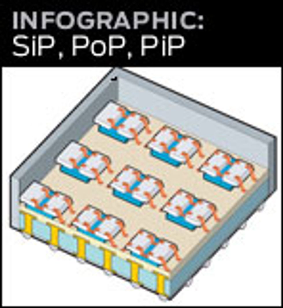
An SiP is a combination of integrated circuits, transistors, and other components (like resistors and capacitors) on two or more die installed within a single package. A graphics processor is a good example. Along with the processing circuitry, it has memory—both dynamic RAM and flash—as well as passive components like resistors and capacitors sitting on top of a single miniature circuit board, and the whole pile goes inside one package. With smart design integration, an SiP may contain multiple and radically different functions—incorporating, for example, microelectromechanical systems, optical components, sensors, biochemical elements, or other devices within that package. It can even contain multiple system-on-a-chip units that combine some of these functions.
Basically, SiP lets designers mix and match components to get higher performance and get their product to market quickly while spending less on R&D, because they’re using existing components. They don’t have to go through a long and expensive design cycle every time they need to add a function; they can simply change part of the collection of die within the package.
The SiP approach can also enable smaller products. We all remember the bulky, single-function video cameras that tourists lugged around years ago. As those cameras got smaller, the sizes of some components—the battery, the lens, and the LCD display, for example—didn’t really change much; people want big displays and lots of power. And the size of a lens is set by its aperture, image sensor, and focal length. So the burden of miniaturization falls on the electronics: When a device shrinks to 66 percent, for example (from 450 cubic centimeters in 2006 to 300 cm3 today), the electronics must shrink to a third or less of their original size.
SiP technology brings another benefit. Data paths between the processor chip and the memory chip are shorter in comparison with those on a circuit board, so data flow is faster and noise is reduced. With less distance to travel, it takes less power to get there—another plus. This reduction in size and increase in performance are the driving forces behind the continued evolution of SiP architectures.
There’s more than one way to build a system-in-a-package. One of them is called package-on-package (PoP). Remember that circuit board crammed with chips? It looks a little like a suburban office park seen from the air. Well, what better way to cram in more office space than to swap out some one-story buildings for multistory replacements? That’s what package-on-package designers are doing. They pack a lot of circuitry into a small volume by stacking one set of connected die on top of another set—flash and DRAM components, for example, on top of an application-specific IC—and then putting them inside a single package so that product designers and manufacturers can deal with them as single units. The sets stack like Lego blocks, typically with logic on the bottom and memory on top. Such structures are adaptable—manufacturers, when necessary, can vary the memory density by swapping out the piece of the stack that holds the memory components, for example. And each of the sets within the package can be tested individually before stacking. After stacking, however, testing becomes more difficult. And manufacturers will worry about possible warping of the miniature circuit boards and die, which would reduce the yield during assembly.
So PoP systems are a little pricey and therefore used only for products whose prices can include a premium for better performance in a smaller, low-power package. Manufacturers of high-end networking products were early adopters of this approach; manufacturers of digital still cameras and cellphones have since joined them. Smartphones and, more recently, tablet computers are using PoPs mainly to integrate application-specific ICs with memory. PoP continues to evolve and will likely migrate into other products further down the consumer-electronics food chain.
Package-in-package (PiP) is another variant of SiP. Instead of just naked die and other components piled onto miniature circuit boards inside a single package, PiP adds packaged die—in other words, chips—into the mix. So PiP puts chips within chips. Semiconductor companies choose this option for business reasons as much as for technical ones—it forces product manufacturers to buy multiple subsystems from the same chip manufacturer. PiP integrates more functions and can improve performance beyond that of PoP systems, but it is less flexible in combining different devices, like memory chips, from different suppliers. It’s also hard to test. In some mobile applications—for example, the most advanced smartphones—manufacturers gladly accept these drawbacks because PiP designs can cram even more into a smaller space. But they haven’t caught on as widely as the PoP approach.
In all these packaging schemes, the most important consideration is the electrical connections between the multiple die and the miniature circuit boards that link them. The traditional and cheapest technology used for these connections is wire bonding, which is in about 80 percent of the packages produced today. Wires connect terminals on an individual chip to the little circuit board inside the package. Then electrical paths on that circuit board route signals among chips and to the leads that extend from the package, enabling it to be connected to other devices within a system.
Despite repeated predictions that wire-bond technology has reached its practical physical limit, it continues to reinvent itself: In the past few years, manufacturers reduced the wire diameter to 15 micrometers to enable them to cram more wire terminals onto the precious real estate of a chip’s surface. They also began changing the wire materials from gold to copper, in response to the skyrocketing cost of gold.
In a conventional wire-bond connection between two chips, the electrical path runs from the closely spaced terminals at the edge of the chip to terminals on the substrate. As the chip shrinks, so does the distance between the individual terminals, and it becomes tricky for designers to avoid short circuits and to keep the wires far enough apart to minimize cross talk.
Nevertheless, many innovations are extending the life of this technology. Some manufacturers, for example, are replacing single rows of wires with multiple rows on the four edges of the chip to give designers more options for electrical paths.
Alternatively, some designers have eliminated the wires altogether and replaced them with “bumps” of solder, gold, or copper. This approach earned the name flip-chip, because the side of the chip with the bumps must be flipped face down to connect with the bumpy side of the chip below or the underlying circuit board. As you can imagine, a small bump of metal is smaller and shorter than a long wire and therefore can conduct a signal much faster and at higher bandwidths. However, this advantage comes at a cost—increasing the overall price of the package to 1.5 to 5 times that of a wire-bond version. Not surprisingly, this technology has also gravitated toward industries that need high performance and will pay for it. It is now standard for high-speed and high-bandwidth microprocessors and graphics processors because of its shorter delay time.
A newcomer to the package scene is the wafer-level chip-scale package. This technology is essentially a package without a package—the naked die has extremely tiny solder balls on its active side, allowing it to connect directly to a circuit board. These die are fragile, so to date this process can be used only for very tiny die, and even these typically need to be further protected with a coating on one side. The vast majority of smartphone manufacturers are beginning to embrace this approach.
Designers have found another way to make SiP devices as small as possible—one that might seem obvious. They simply make the wafer thinner—taking a wafer that is, say, a little over 700 µm thick and reducing it to perhaps 100 or even 50 µm or less. Because the size of the wafer eventually determines the size of the package, and therefore the size of that device you’re carrying in your pocket, that change can make a big impact.
Mechanical grinding is the most popular way to thin a wafer. It’s just what you’d expect: Manufacturers physically grind the wafer down, typically by rolling it through a slurry of water and abrasive particles or rubbing it with diamond particles embedded in a resin. There are lots of other ways to thin a wafer, including chemical mechanical polishing, which smooths surfaces with the combination of chemical and mechanical forces, and chemical etching, which uses chemical liquids or vapors to remove some of the wafer material.
With the trend toward smaller packages, manufacturers are making die thinner than was ever thought possible. For example, one manufacturer recently privately demonstrated a flash memory die 10 µm thick and a tiny RF device measuring 50 by 50 by 5 µm.
SiPs are the best way to pack very different functions into a single electronic device. In the future, the individual pieces in an SiP could be as diverse as RF antennas, photodiodes, and drug delivery tubes—perhaps even a protein layer that could allow the chip to connect with human tissue.
But we’re not quite there yet. Putting such complex devices into a single package will require new materials and control of their interactions on the nanometer scale—and perhaps even on the molecular scale. It won’t be easy. There will be tough competition as consumers demand smaller and smaller devices that do more and more. Designers are now investigating taking packageless packaging beyond simply attaching naked die to circuit boards; they are beginning to attach naked die directly to each other in three dimensions. Some manufacturers are already making simple versions of these 3-D modules, but this technology has a long way to evolve before it can become a staple of the manufacture of high-volume commercial products.
All these packaging innovations are remarkable, but the real impact has to be measured by what they enable in the real world—and how they will change society. Electronics are woven into the fabric of our lives and are beginning to be woven, literally, into the clothes we wear. Increasingly, they will be implanted in our bodies as well. Pacemakers, defibrillators, and microfluidic pumps for drug delivery are in use; biosensors and other implantable devices that can send data to external computers are on the way. Devices that may allow control of epilepsy, Parkinson’s disease, and migraines are already in clinical trials. Future forms of packaging will not only have to protect the electronics from the environment but also shield a sensitive environment—the human body—from the electronics. These innovations will improve our work, our health, our play, and even our longevity.
This article originally appeared in print as “Good Things in Small Packages.”
About the Authors
Pushkar Apte, W.R. Bottoms, William Chen, and George Scalise worked on the International Technology Roadmap for Semiconductors, which among other things covers future packaging technology, the focus of “Good Things in Small Packages.” Apte, now a consultant, was vice president of technology at the Semiconductor Industry Association, where Scalise was president before retiring this year. Bottoms, with over 30 years in the industry, was most recently chairman of Third Millennium Test Solutions. Chen, a three-decade IBMer, is now a fellow for the ASE Group.