Currently, wireless optical communication on computer chips occurs at near-infrared wavelengths. But if visible light could be used in these on-chip optical communications, the chips could be miniaturized significantly because the wavelengths in that portion of the spectrum are much smaller.
Now researchers at Boston College have developed a nanoscale wireless communication system that does just that. The key to the technology, as described in the journal Nature Scientific Reports, are antennas that can collect photons and reversibly convert them into surface plasmons with a high degree of control.
Surface plasmons are the oscillations in the density of electrons that occur when photons hit a metallic surface. The field that exploits this physical phenomenon is known as plasmonics.
This new nanoantenna is not the first of its kind. But it represents a new wrinkle the Boston College researchers brought to the game: the ability to herd the photons onto a single path, which allows what is known as in-plane communication. The gist of it is that a two-way transmission of information occurs across a single line of photons. Previously, keeping the emission and collection of the electromagnetic radiation collated along a single path was exceedingly difficult. Overcoming this hurdle is a critical step toward enabling high-speed communication in on-chip systems.
"We have developed a device where plasmonic antennas communicate with each other with photons transmitting between them," said Michael J. Naughton, a professor at Boston College who led the research, in a press release. "This is done with high efficiency, with energy loss reduced by 50 percent between one antenna and the next, which is a significant enhancement over comparable architectures."
The researchers claim that the device they have developed could make the transmission of data as much as 60 percent faster than earlier plasmonic wave-guide techniques, and up to 50 percent faster than plasmonic nanowire wave guides.
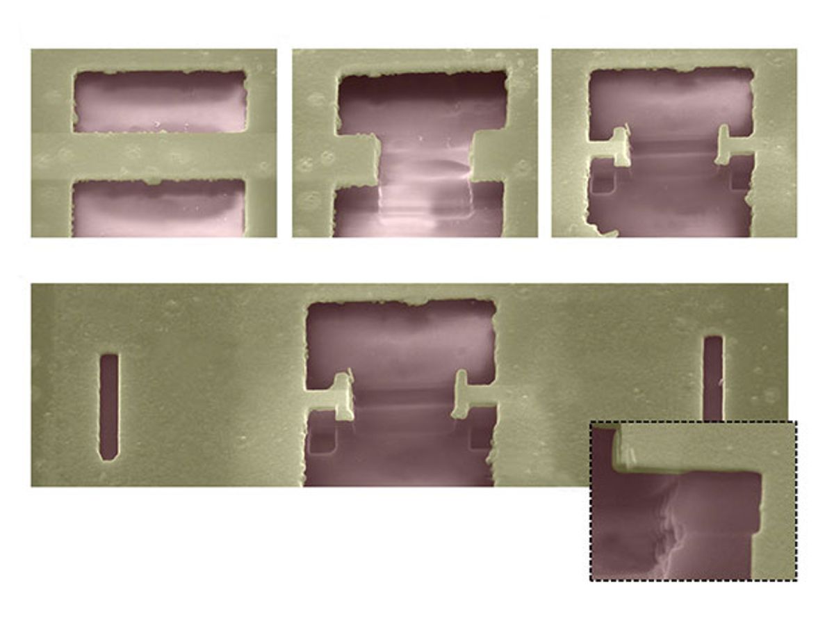
One of the keys to making the device so much faster was the inclusion of a small gap of air between the waves and the metal surface of the device. The researchers created this air gap by removing a small bit of the glass substrate, which reduced the disruptive pull of the material on the photons during transmission. The researchers are able to tune the device by either widening or narrowing the air gap.
The researchers have already shown that the device can outperform silicon-based optical wave guides that currently support on-chip optical transmission, mainly because the transmission of data is not slowed down by the dispersion of light that occurs in these wave guides. Instead, the surface plasmons travel at 90 to 95 percent the speed of light while the photons travel at light speed.
Juan M. Merlo, the postdoctoral researcher who initiated the project, added: “Silicon-based optical technology has been around for years. What we are doing is...developing a tool to make silicon photonics faster and greatly enhance rates of communication."
Dexter Johnson is a contributing editor at IEEE Spectrum, with a focus on nanotechnology.


