Silicon has been the mainstay of chips for much of their history (a history you can explore in IEEE Spectrum’s Chip Hall of Fame). This is in large part because silicon possesses a “Goldilocks” band gap of 1.1 electron Volts (eV), which makes it possible to operate integrated circuits at a low voltage, leading to reduced leakage of current.
Another key feature of silicon is that it can be used to make a convenient “native” insulator, in the form of silicon oxide. Silicon oxide managed to serve as an insulator for silicon circuits for many generations of chips, isolating components and reducing gate leakage currents, until high-K dielectrics took over the job a decade ago.
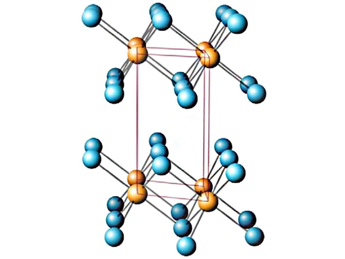
Now researchers at Stanford University and SLAC National Accelerator Laboratory have found that some of the most sought after high-K materials—namely hafnium selenide (HfSe2) and zirconium selenide (ZrSe2)—possess the same perfect band gap seen in silicon when they are thinned down to two-dimensional (2D) materials. As a result, the Stanford researchers have discovered a 2D material version of the handy silicon/silicon dioxide combination that enabled generations of chip designs. But in this case the combination can be shrunk down ten times smaller.
In research described in the journal Science Advances, the Stanford scientists found that when the well-known and desirable high-K dielectrics HfSe2 and ZrSe2 were thinned down to a single layer—about three atoms thick—they sustained a moderate band gap of about 1 eV. This stands in stark contrast to silicon and other “bulk” 3D semiconductors that begin to suffer decreases in their carrier mobility, as well as increases to their band gap, when they are thinned down below about 5 nanometers.
“We fabricated several devices (transistors),” said Eric Pop, Associate Professor at Stanford and co-author of the research, in an e-mail interview with IEEE Spectrum. “The high-K dielectric acts as both the gate dielectric and a passivation layer against traps and defects. In other words, the ‘native’ high-K dielectric gives an improved semiconductor interface for the transistor operation.”
The typical metal–oxide–semiconductor field-effect transistor (MOSFET) forms the basic building block of most modern intergrated circuits. It is comprised of a gate, source, and a drain. MOSFETs are basically a switch in which a voltage from the gate turns on or off a flow of current between the source and the drain.
The design of MOSFETs for a long time involved putting an insulating layer on the surface of the semiconductor and then placing a metallic gate electrode on top of that. The thin layer of insulation electrically isolates the transistor’s gate from the channel through which current flows when the transistor is on. Silicon served as the semiconductor and silicon oxide was the insulator. But as chip dimensions continued to shrink, silicon oxide had to be made so thin it was no longer an effective insulator, at which point the industry turned to high-K dielectrics.
The “K” represents the dielectric constant, which refers to a material’s ability to concentrate an electric field. When an insulator has a higher dielectric constant, it can provide increased capacitance between two conducting plates—storing more charge—for the same thickness of insulator.
While high-K dielectrics have helped to overcome insulator issues as chips have continued to shrink, these materials are not “native” on silicon (only silicon dioxide is). As a result, another “buffer” layer (like silicon dioxide) is still required before deposition in order to handle the mismatch between the atomic structure of each material.
“By having a native high-K dielectric, especially combined with a 2D material, one could design extremely thin (~nanometer) transistors which consequently can also be made very short (in terms of gate length),” said Pop. “The high-K dielectric also ensures that lower-voltage operation is possible for such transistors. We estimate that with these 2D materials, the shortest transistors would be about ten times smaller than what is possible with silicon, even with silicon and high-K.”
In order for this approach to actually become a commercial solution, the HfSe2 and ZrSe2 films would need to be scaled up to large-area wafers, with uniform thickness and crystallinity, according to Pop. In addition, greater control would be needed of the oxidation step (or any additional oxide deposition), ensuring good uniformity, high quality insulating high-K dielectrics.
Pop added: “Finally, we would need improved electrical contacts to such transistors. This is unsurprising, as making good-quality electrical contacts is challenging to any ultra-thin material, including other 2D materials or very thin silicon.”
Dexter Johnson is a contributing editor at IEEE Spectrum, with a focus on nanotechnology.


