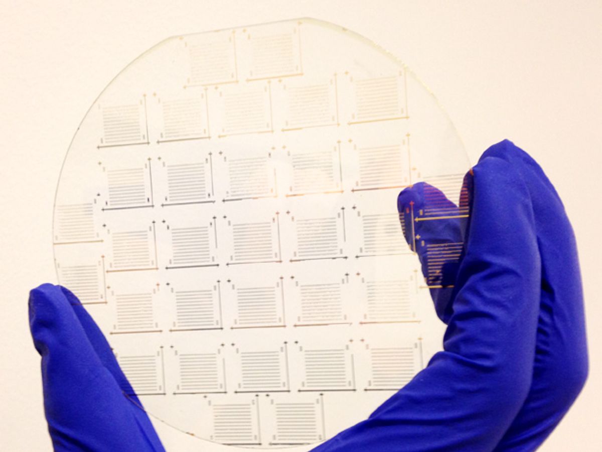
Researchers at Cornell University have developed a process for producing transition metal dichalcogenides (TMDs) with spatial uniformity—a key attribute for thin films in electronics—on wafers. This development could ultimately translate into atomically thin semicondutor layers that could pave the way for atomic-scale minutarization of electronics.
TMDs are made up of materials that combine one of 15 transition metals, such as molybdenum or tungsten, with one of the three members of the chalcogen family: sulfur, selenium or tellurium. Researchers have investigated only a small number of the possible combinations of these TMD materials for electronic applications. So far, the leaders of the class are tungsten diselenide (WSe2) and the ever more popular molybdenum disulfide (MoS2).
While TMDs exhibit great promise in electronic applications, commercial viablity depends on developing a process to grow them wafers. Exfoliation and chemical vapor deposition (CVD) methods have proved inadequate either because of poor scalability or contamination.
The Cornell researchers tweaked a process called metal organic chemical vapor deposition (MOCVD) that uses molecular precursors to introduce and precisely control the amount of transition metal atoms (molybdenum or tungsten) and chalcogen atoms.
“Since these metal organic molecules are used in its gas phase, we can control its concentration (partial pressure) very well,” explained Jiwoong Park, a professor at Cornell and one of the researchers, in an e-mail interview with IEEE Spectrum. “The MoS2 and WS2 monolayers were successfully grown on various insulating substrates, including silica, oxidized silicon wafer, silicon nitride, etc.”
Previously, transition metal was introduced using solid phase sources such as evaporated molybdenum metal or oxide (MoO3), but controlling the amount of the metal atoms in the growth chamber was very difficult. By using MOCVD, the researchers were able to overcome this limitation.
Tobin Marks and Mark Hersam of Northwestern University (Hersam’s work with 2-D materials we have covered in this blog) point out in Nature News that the Cornell researchers employed this MOCVD process to produce a 99% device yield for field-effect transistors. While the electron mobility of the devices was good for TMDs at 30 square centimeters per volt per second, Marks and Hersam say that this electron mobility is still ten times smaller than what can be attained with bulk crystalline silicon.
Nonetheless, this latest work has demonstrated a process that is fully scalable for applying TMDs to wafers and shows an encouraging way forward for the use of these materials in electronics and optoelectronics.
“One can consider our material as three-atom-thick semiconductor wafer grown on top of another insulating substrate,” said Park. “Conventional photo and e-beam lithographic techniques can be used directly to make a large array of high performance electronic and optoelectronic devices.”
Dexter Johnson is a contributing editor at IEEE Spectrum, with a focus on nanotechnology.


