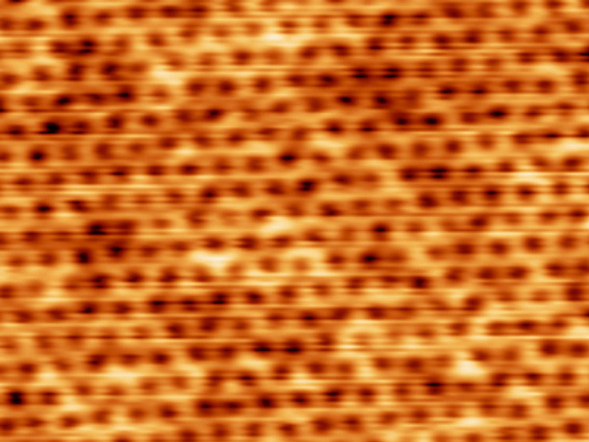
When you hear people sing the praises of graphene, they are usually referring to the single-crystal graphene that has many attractive properties like high electron mobility. Unfortunately, producing that pure single-crystal graphene requires a decidedly unscalable method known as the “Scotch Tape” method; graphene is pulled off in single-layer flakes directly from bulk graphite.
Chemical Vapor Deposition (CVD) has been seen as a bridge between scalability and purity in graphene production. With that technique, graphene is grown on a metal substrate like copper or nickel. But because the graphene eventually has to be peeled off of the metal substrate, the graphene can either be completely ruined or contaminated.
Now researchers at the University of Groningen in the Netherlands have devised a production method based on CVD that eliminates the potential for ruin or contamination while still remaining scalable. It is based on something they discovered when analyzing CVD-grown graphene three years ago.
“When we analyzed a sample of graphene on copper, we made some strange observations,” said Meike Stöhr, one of the researchers, in a press release.
What the researchers observed was that some copper oxide was present next to the copper. In fact, the graphene formed a kind of film on top of the copper oxide. Because oxidized metals are often used in passivation of electronics—a process in which a light coat of a protective oxide is used to create a shell against corrosion—the researchers suspected that the copper oxide layer could leave the graphene’s properties untouched.
In research published in the journal Nano Letters, the Groningen researchers took their initial observations and demonstrated the ability to grow graphene on copper oxide. Most importantly, the process of decoupling the graphene and copper oxide preserves the graphene’s attractive electronic properties.
While Stöhr concedes that their work will need to be duplicated by other research groups, their findings could have a long-reaching impact on the future of graphene devices. If this process enables the growth of large single-domain crystals of graphene, it would be possible to then use common lithographic techniques to etch a host of electronic devices in a way analogous to silicon.
Dexter Johnson is a contributing editor at IEEE Spectrum, with a focus on nanotechnology.


