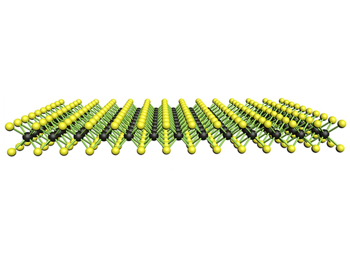
Layered two-dimensional (2D) transition metal dichalcogenides (TMDs)—like tungsten disulfide or molybdenum disulfide—are attractive for electronics applications because you can manipulate their band gap simply by adjusting the number of layers used.
But there’s a catch: it’s tricky to develop a processes that will lead to large-area synthesis of device quality TMDs. Now researchers at New York University’s (NYU) Tandon School of Engineering may have taken a big step toward closing down this issue with a new manufacturing process for tungsten disulfide that resulted in highest quality ever reported for the material.
In research described in Applied Physics Letters, the scientists made some variations on the process known as chemical vapor deposition (CVD). In CVD, gaseous reactants are introduced into a furnace to form a film on a metal substrate that’s usually made of copper. The material then “grows” on the substrate. To spur that growth intungsten disulfide, salt molecules are added to act as seed layer. Unfortunately, these seed layers lead to impurities in the final material. So the NYU team developed a seedlesss growth process.
“We made some subtle and yet critical changes to improve the design of the reactor and the growth process itself, and we were thrilled to discover that we could produce the highest quality monolayer tungsten disulfide reported in the literature,” said Davood Shahrjerdi, in a press release. “It’s a critical step toward enabling the kind of research necessary for developing next-generation transistors, wearable electronics, and even flexible biomedical devices.”
In an e-mail interview with IEEE Spectrum, Shahrjerdi explained that the resulting tungsten disulfide provided a large energy bandgap (2.0 electron volts). Its charge carriers also had a small effective mass: the smaller the effective mass the higher the carrier mobility. “The carrier mobility of our film is 2-3 times better than the best reports in the literature,” said Shahrjerdi.
The material also exhibited strong spin-orbit coupling, an interaction between a particle’s spin and its motion that is important for making spin-based devices, or spintronics.
The NYU team fabricated transistors from the materials and used them for measuring the carrier mobility. In future, the researchers are looking to build flexible electronics.
“Previously, we have demonstrated high-performance flexible electronics based on nanoscale silicon integrated circuits and high-efficiency III-V solar cells on plastic substrates,” said Shahrjerdi. “The atomic layer thickness of these 2D materials makes them suitable for flexible applications.”
Shahrjerdi said that his team also plans to develop high-speed radio frequency transistors and circuits based on the tungsten disulfide they have synthesized.
Dexter Johnson is a contributing editor at IEEE Spectrum, with a focus on nanotechnology.


