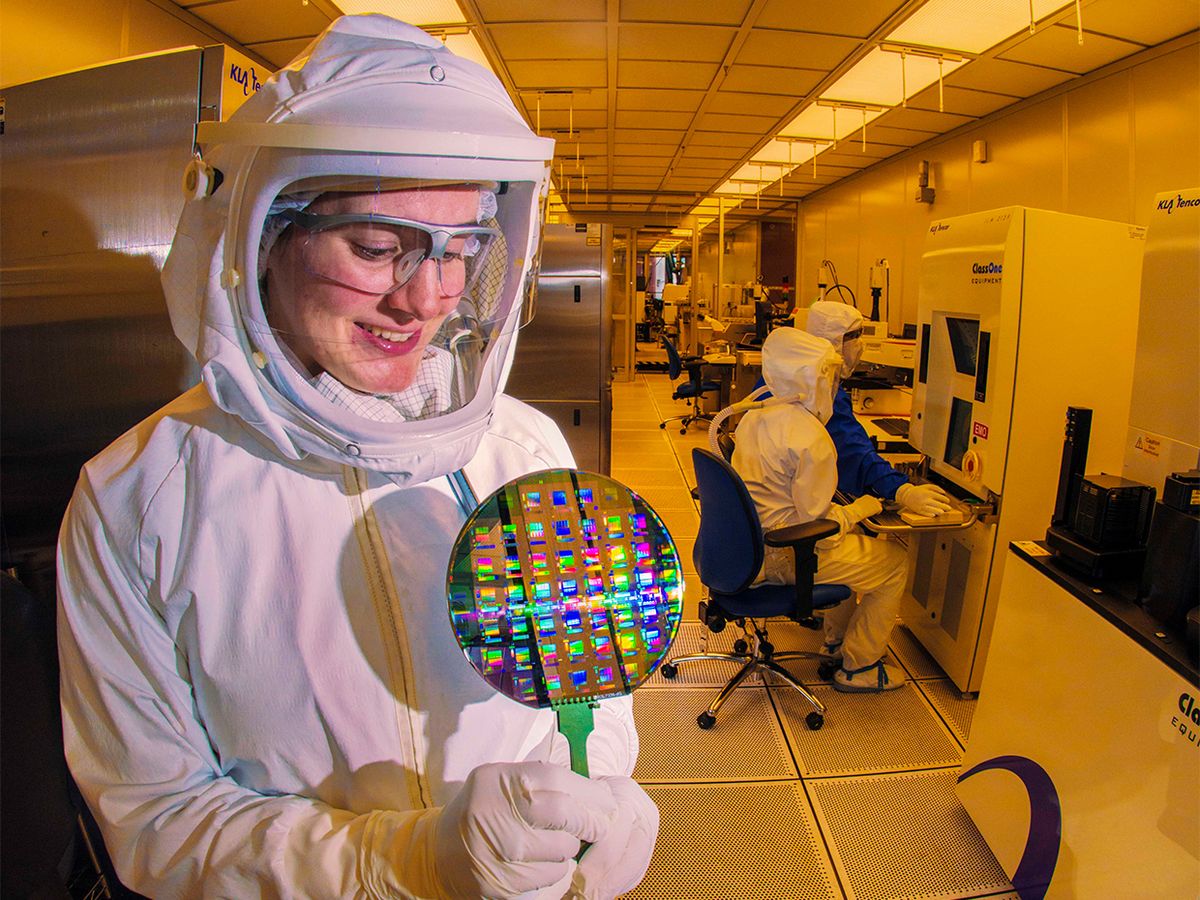
The U.S. is investing in upgrades to the fabrication facility that makes the radiation-hardened chips for its nuclear arsenal. It is also spending up to US $170-million to enhance the capabilities of SkyWater Technology Foundry, in Bloomington, Minn., in part to improve the company’s radiation-hardened-chip line for other Defense Department needs.
The fab that makes the chips for U.S. nuclear weapons is both super-advanced and kind of antiquated. The MESA fab at the Energy Department’s Sandia National Laboratories in New Mexico makes chips that can compute through a blaze of radiation and do so reliably for decades. But it operates using a 350-nanometer manufacturing process, a geometry Intel pioneered back in 1994. And it uses that process to build chips on 150-millimeter silicon wafers, a size that began to lose position that same year.
200-mm wafers allow more chips to be made on a single wafer than on 150-mm wafers, reducing cost. But that wasn’t the primary motivation for an upgrade, explains Michael Holmes, senior manager of microfabrication at MESA. “For us, this conversion is not so much about volume as supply chain. It’s about access to tools and spare parts and raw materials,” he says. Tools designed for 150-mm wafers and the parts needed to maintain those tools are becoming are more difficult to source. Though the most advanced fabs and foundries have been using 300-mm wafers for more than a decade, 200-mm wafer facilities are still plentiful and there is an industry for equipping them.
MESA has completed the first of a four-phase conversion process that involves rebuilding chemical recipes, adjusting hundreds of process parameters, and extensive testing. All of that has to go on while the fab is producing chips using the old process. Holmes says the transition will be complete in time for a customer use to use the new process in July 2021.
At the same time, MESA is embarking on a separate upgrade that will result in a 180-nm radiation hardened process technology, which will essentially double the density of transistors on nuclear weapons chips. “In our mission space, while high reliability and radiation hardening are our primary requirements, we also need to scale this technology to provide denser and more complex logic function,” says Holmes.
Separately, the Defense Department is providing up to $170-million to SkyWater Technology Foundry to develop a 90-nanometer process for radiation hardened chips and to add the capability of producing copper interconnects. The requirements for the resulting chips are less stringent than those for chips coming out of Sandia’s MESA facility, but they will be useable in the critical systems of other military gear and in space.
The radiation-hardening process relies on what’s called partially depleted silicon-on-insulator (SOI) technology. It involves the use of a silicon wafer that has a layer of oxide buried below the transistor layer. SOI chips are inherently more tolerant of radiation than ordinary silicon chips. When radiation strikes silicon, it can create mobile charge that interferes with the chip’s operation. However, in an SOI chip, the oxide layer prevents radiation-induced charge from getting into the transistor layer. SkyWater will present its radiation hardened process on 6 November at the Radiation Hardened Electronics Technology conference in Melbourne, Fla.
In addition to the radiation-related upgrade, SkyWater is expanding its interconnect-manufacturing capabilities with an eye to moving another notch up the Moore’s Law ladder. SkyWater currently uses a 90-nanometer silicon technology with aluminum interconnects. About 15 years ago, the higher-end of the industry moved from aluminum to copper, which is less resistive, in order to increase chips’ energy efficiency. The addition of copper will let SkyWater produce high-end mixed signal chips for IoT devices as well as silicon interposers for chiplets and advanced packages. “The addition of copper interconnects represents an important material processing capability that SkyWater needs to support node scaling to 65 nm and 45 nm, and aligns with our customers’ technology roadmaps,” says the company’s chief technology officer Brad Ferguson.
The combined development will involve a 5500-square-meter expansion of the foundry and a 30- to 50-person increase in headcount, according to the company. The funding’s initial phase, for the radiation hardened circuits work, is $80-million. SkyWater is already involved in a $61-million program to develop 3D carbon nanotube-based chips.
Samuel K. Moore is the senior editor at IEEE Spectrum in charge of semiconductors coverage. An IEEE member, he has a bachelor's degree in biomedical engineering from Brown University and a master's degree in journalism from New York University.


