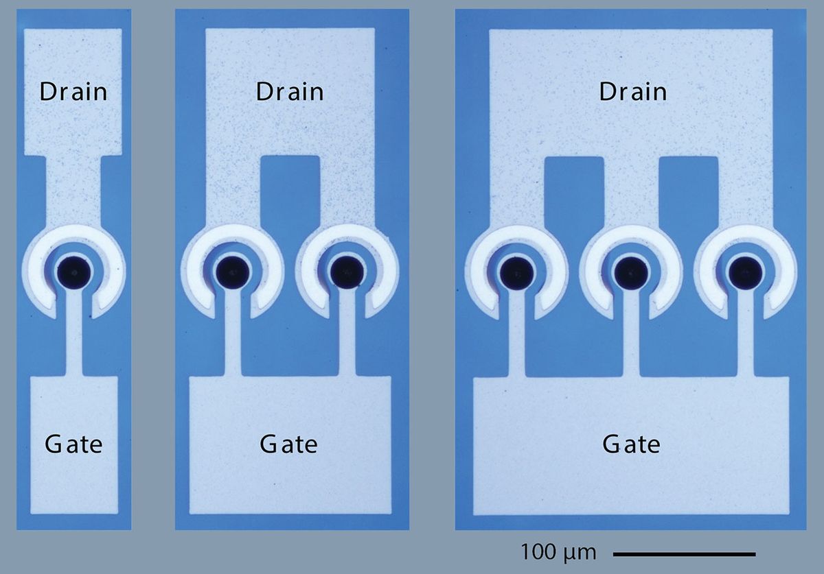
Through-silicon vias (TSVs) are the standard way to stack chips these days. They're basically micrometer-scale vertical wires embedded in a sliver of silicon that link one chip, such as a processor, to another, such as a memory chip, stacked atop the first. That way signals don’t have to travel very far between the two chips. Done right, they should save time, energy, and space. But, at the moment, they don’t add any intelligence.
Engineers in Germany want to change that by making TSVs smart. Their answer is a “through-silicon transistor,” and if they’re right, it should let designers actively control which signals are allowed to go from one chip to another. The implications aren’t just more intelligent control of the flow of information—through-silicon transistors could also keep sensitive chip designs safe from prying (electron-microscope enhanced) eyes.
Felix Winkler, a Ph.D. student at Technische Universität Dresden, in Germany, and his colleagues in the laboratory of Johann W. Bartha started with a thick sliver of silicon, called an interposer. Ordinarily when making a TSV, manufacturers etch narrow holes through the interposer and fill them with copper. Instead, Winkler and his colleagues turned the hole into a field-effect transistor (FET).
To understand how, you need to know the basic parts of a FET. A FET has four main components: the source, the drain, the channel between them, and the gate, which sits above the channel but is separated from it by a thin layer of insulation. Depending on the pattern of chemicals with which the different parts have been impregnated, voltage at the gate either allows current to flow through the channel between the source and drain, or it cuts off the flow of current.

In the through-silicon via field effect transistor (TSVFET), the drain and source were at the top and bottom of the hole, which was 20 micrometers wide and 200 micrometers deep. The gate lines the hole itself. So when Winkler applied voltage to the gate, current flowed from top to bottom through the area surrounding the hole.
“You can easily, just by applying a voltage or taking it off, activate a chip or deactivate it completely,” says Winkler.

Winkler adds that the TSVFETs can be linked up to form elementary circuits such as inverters or even an SRAM memory cell. In addition to adding some control electronics within the interposer, the TSVFET could act as a kind of camouflage to prevent the reverse engineering of a chip or to keep contract manufacturers from producing systems on the sly.
Chip designers fear that a foundry contracted to make 1 million chips for a designer might instead make 2 million and secretly sell the other half themselves, explains Winkler. Processors and other complex chips usually have a dozen or more layers of copper interconnects to link the transistors in the silicon together to form circuits. So one solution is to have one foundry build the bottom layers of interconnect and another build the top layers. That way neither manufacturer has the whole design.
But a smart interposer, powered by TSVFETs, might be a simpler solution, Winkler argues. One manufacturer could produce all the interconnect layers so long as a different one built the interposer. With its TSVFET-powered logic, the interposer would form a final fail-safe of connections, without which the system wouldn’t work.
Winkler is hoping that other ideas will come up, now that the concept has gotten an airing in IEEE Electron Device Letters. In the meantime, the TU Dresden team will figure out the frequency limits of the transistor and experiment with having different dimensions from the 200-micrometer by 20-micrometer versions they built.
Samuel K. Moore is the senior editor at IEEE Spectrum in charge of semiconductors coverage. An IEEE member, he has a bachelor's degree in biomedical engineering from Brown University and a master's degree in journalism from New York University.


