The Conversation (0)

Photo: Dan Saelinger
In 2018, an article in Bloomberg Businessweek made the stupendous assertion that Chinese spy services had created back doors to servers built for Amazon, Apple, and others by inserting millimeter-size chips into circuit boards.
This claim has been roundly and specifically refuted by the companies involved and by the U.S. Department of Homeland Security. Even so, the possibility of carrying out such a stupendous hack is quite real. And there have been more than a dozen documented examples of such system-level attacks.
We know much about malware and counterfeit ICs, but the vulnerabilities of the printed circuit board itself are only now starting to get the attention they deserve. We’ll take you on a tour of some of the best-known weak points in printed-circuit-board manufacturing. Fortunately, the means to shore up those points are relatively straightforward, and many of them simply amount to good engineering practice.
In order to understand how a circuit board can be hacked, it’s worth reviewing how they are made. Printed circuit boards typically contain thousands of components. (They are also known as printed wiring boards, or PWBs, before they are populated with components.) The purpose of the PCB is, of course, to provide the structural support to hold the components in place and to provide the wiring needed to connect signals and power to the components.
PCB designers start by creating two electronic documents, a schematic and a layout. The schematic describes all the components and how they are interconnected. The layout depicts the finished bare board and locates objects on the board, including both components and their labels, called reference designators. (The reference designator is extremely important—most of the assembly process, and much of the design and procurement process, is tied to reference designators.)
Not all of a PCB is taken up by components. Most boards include empty component footprints, called unpopulated components. This is because boards often contain extra circuitry for debugging and testing or because they are manufactured for several purposes, and therefore might have versions with more or fewer components.
Once the schematic and layout have been checked, the layout is converted to a set of files. The most common file format is called “ Gerber,” or RS-274X. It consists of ASCII-formatted commands that direct shapes to appear on the board. A second ASCII-formatted file, called the drill file, shows where to place holes in the circuit board. The manufacturer then uses the files to create masks for etching, printing, and drilling the boards. Then the boards are tested.
Next, “pick and place” machines put surface-mount components where they belong on the board, and the PCBs pass through an oven that melts all the solder at once. Through-hole components are placed, often by hand, and the boards pass over a machine that applies solder to all of the through-hole pins. It’s intricate work: An eight-pin, four-resistor network can cover just 2 millimeters by 1.3 mm, and some component footprints are as small as 0.25 mm by 0.13 mm. The boards are then inspected, tested, repaired as needed, and assembled further into working products.
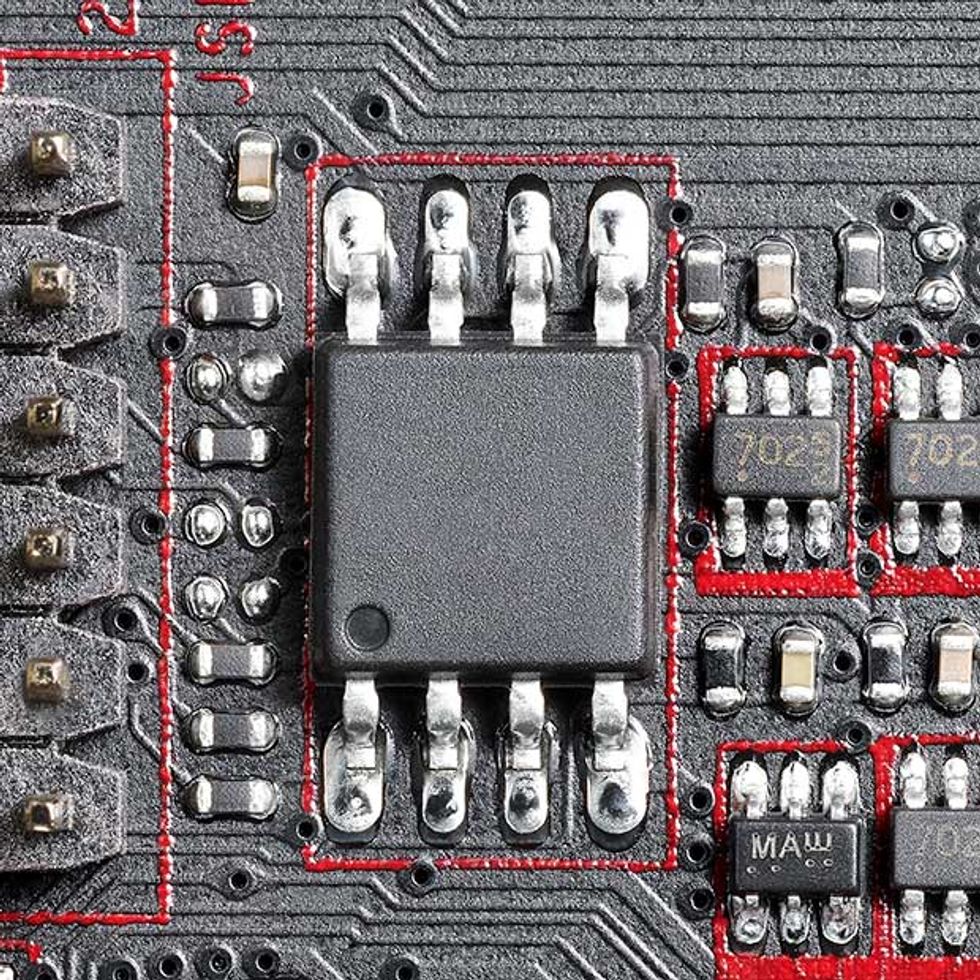
Five Tempting Targets
Hacking a PCB likely means making secret additions to the many small components on a board and taking control of certain data buses
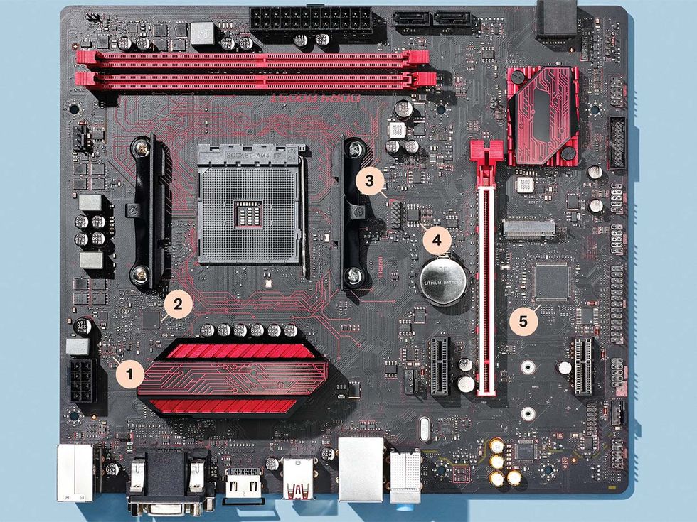
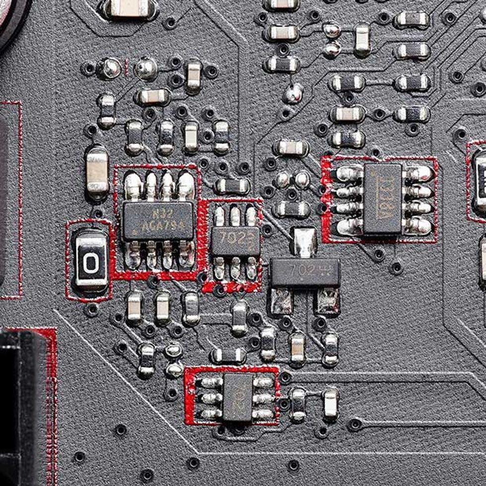
1. Small Components: Hardware hacks might need the inclusion of an extra, surreptitious component. In that case, a spot on the board with many small components is the place to hide it. Modern passive components can be mere millimeters in size and invisible to the unassisted eye. This component can be added in production (very difficult); during the “rework” step, when faulty boards are fixed (easier); or in a warehouse before or during delivery to the customer (even easier).
2. Power Controller: This chip is a particularly fruitful target because it acts as the controller for all of the DC voltages that power the CPU, the graphics card, and more. It is under the control of the System Management Bus. So if a hack enables people to seize control of the SMBus, they could reset voltages in order to damage a computer or limit its operation. Control of the SMBus could also allow a hacker to interfere with communication between the CPU and onboard sensors, and that might also lead to damage.
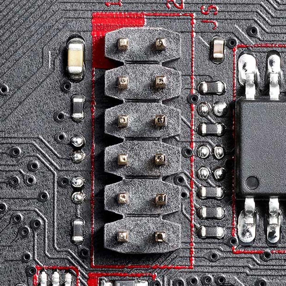
3. Low Pin Count Bus: The connector above is attached to the LPC bus, which can link the CPU to certain legacy devices as well as to the fans and physical switches on the chassis. Perhaps just as important to hackers, the LPC bus can connect to a secure microcontroller called a Trusted Platform Module (TPM), which deals with encryption keys and various other security functions. While the TPM would very likely remain secure even if the LPC bus is compromised, a hacker could observe the traffic going to and from the TPM.
4. BIOS Flash Memory: The Basic Input/Output System (BIOS) flash memory holds the data needed to initialize hardware during boot up. It sits on the Serial Peripheral Interface (SPI) bus. Seizing control of the SPI bus would enable a hacker to alter hardware configurations so that a path would be open to inserting malicious code into the computer.
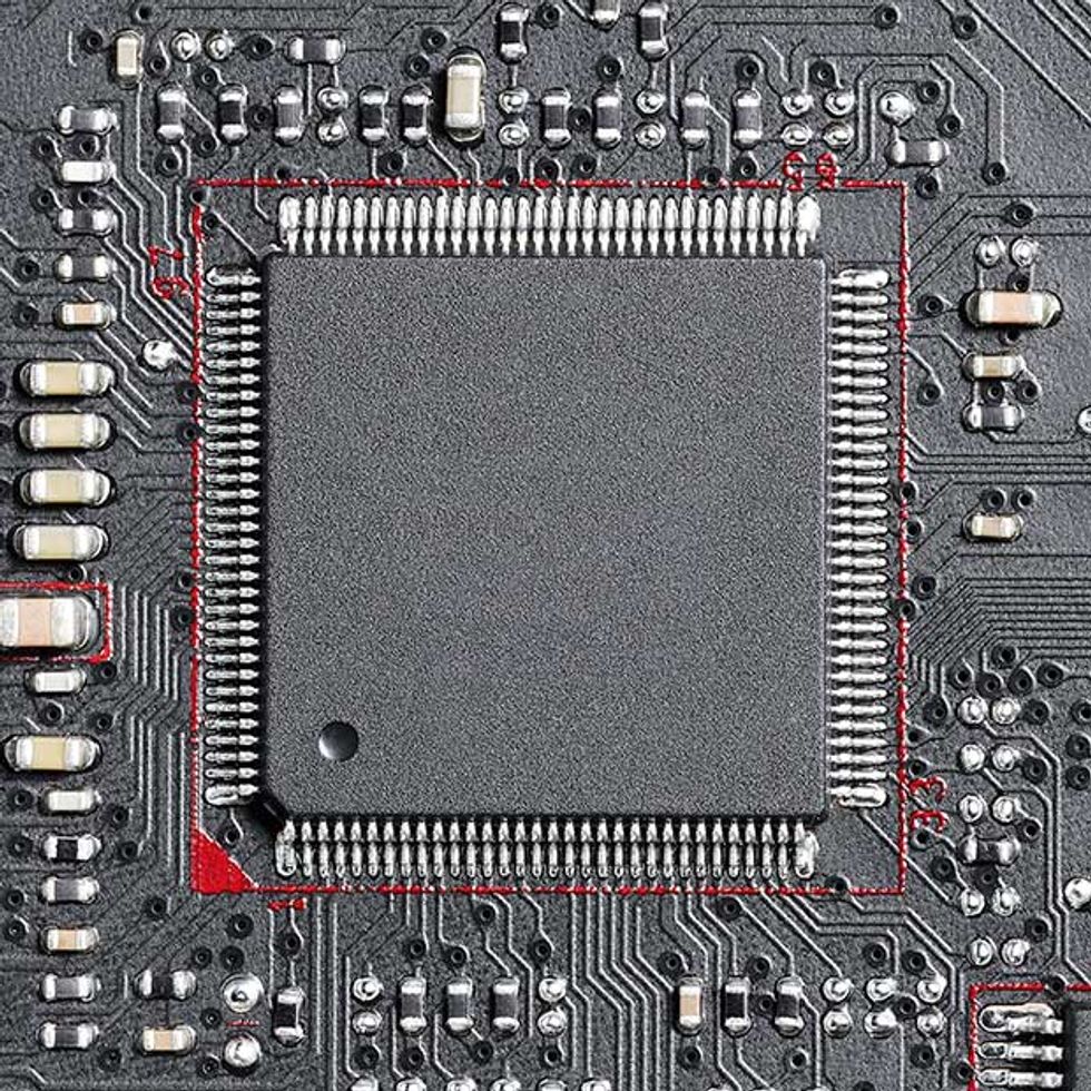
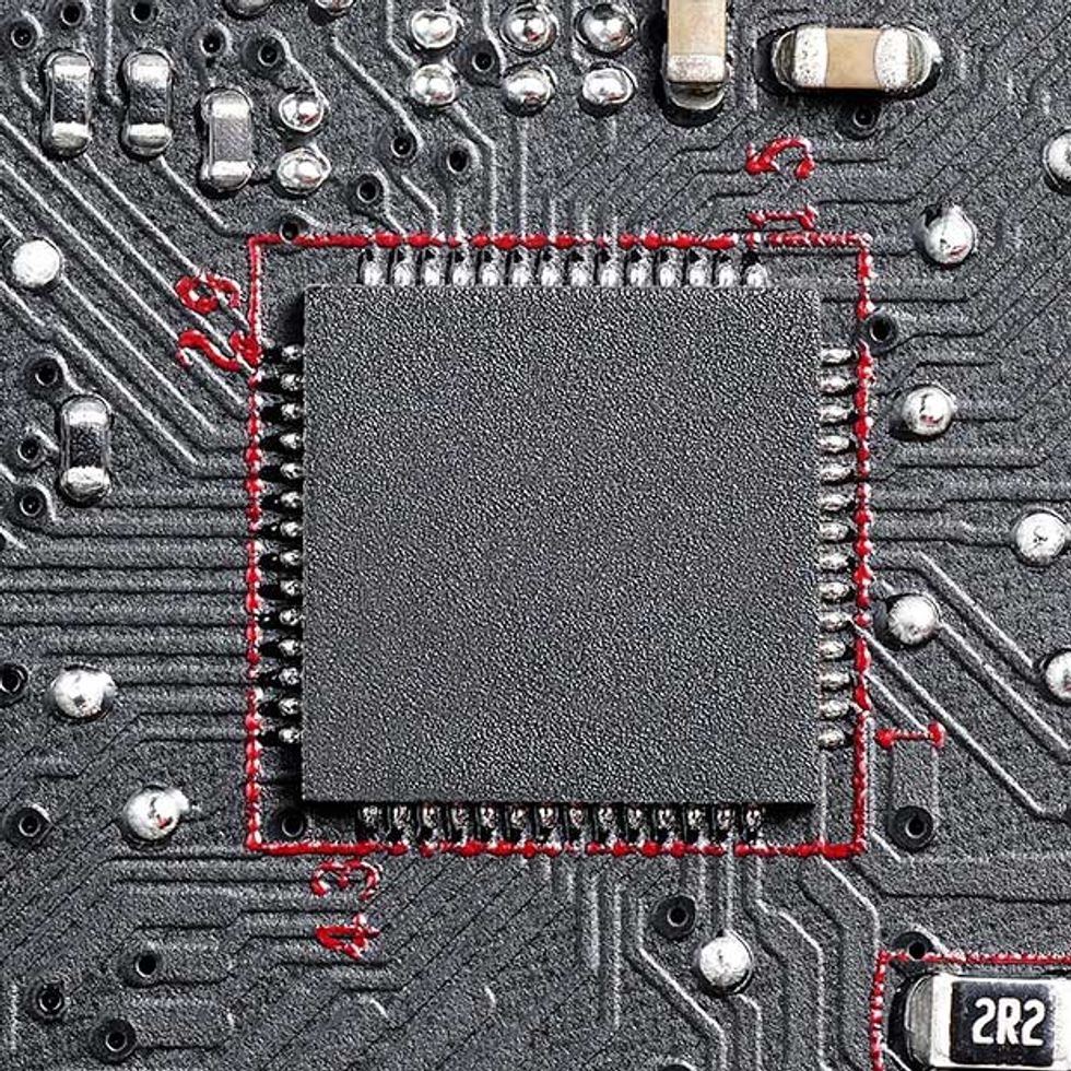
5. Super I/O Chip: The Super I/O chip controls the inputs to a variety of low-bandwidth devices, sometimes including keyboards, the mouse, certain sensors, fans, and floppy disks. The chip sits on the Low Pin Count (LPC) bus. Seizing control of the LPC bus could let hackers reduce the fan speed so that a computer will overheat. It could also let them introduce false temperature and voltage readings that could damage or shut the system down.
Attacks can be made at every one of these design steps. In the first type of attack, extra components are added to the schematic. This attack is arguably the hardest to detect because the schematic is usually regarded as the most accurate reflection of the designer’s intent and thus carries the weight of authority.
A variation on this theme involves adding an innocuous component to the schematic, then using a maliciously altered version of the component in production. This type of attack, in which seemingly legitimate components have hardware Trojans, is outside the scope of this article, but it should nevertheless be taken very seriously.
In either case, the countermeasure is to review the schematic carefully, something that should be done in any case. One important safeguard is to run it by employees from other design groups, using their “fresh eyes” to spot an extraneous component.
In a second type of attack, extra components can be added to the layout. This is a straightforward process, but because there are specific process checks to compare the layout to the schematic, it is harder to get away with it: At a minimum, a layout technician would have to falsify the results of the comparison. And combatting this form of attack is simple: Have an engineer—or, better, a group of engineers—observe the layout-to-schematic comparison step and sign off on it.
In a third type of attack, the Gerber and drill files can be altered. There are three important points on the Gerber and drill files from a security perspective: First, they’re ASCII-formatted, and therefore editable in very common text-editing tools; second, they’re human-readable; and third, they contain no built-in cryptographic protections, such as signatures or checksums. Since a complete set of Gerber files can be hundreds of thousands of lines, this is a very efficient mode of attack, one that is easily missed.
In one example, an attacker could insert what appears to be an electrostatic discharge diode. This circuit’s design files are made up of 16 Gerber and drill files. Of the 16 files, nine would need altering; of those nine, seven would vary in a total of 79 lines, and two files need changes in about 300 lines each. The latter two files specify the power and ground planes. A more skilled attack, such as one adding vertical connections called vias, would dramatically reduce the number of lines that needed rewriting.
Unprotected Gerber files are vulnerable to even a single bad actor who sneaks in at any point between the designing company and the production of the photolithographic masks. As the Gerber files are based on an industry standard, acquiring the knowledge to make the changes is relatively straightforward.
One might argue that standard cryptographic methods of protecting files would protect Gerber files, too. While it is clear that such protections would guard a Gerber file in transit, it is unclear whether those protections hold when the files reach their destination. The fabrication of circuit boards almost always occurs outside the company that designs them. And, while most third-party manufacturers are reputable companies, the steps they take to protect these files are usually not documented for their customers.
One way to protect files is to add a digital signature, cryptographic hash, or some other sort of authentication code to the internal contents of the file in the form of a comment. However, this protection is effective only if the mask-making process authenticates the file quite late in the process; ideally, the machines that create the photolithography masks should have the ability to authenticate a file. Alternatively, the machine could retain a cryptographic hash of the file that was actually used to create the mask, so that the manufacturer can audit the process. In either case, the mask-making machine would itself require secure handling.
Knowing how to sabotage a PC is only half the job. Attackers also have to know what the best targets are on a computer motherboard.
If bad actors succeed at one of these three attacks, they can add an actual, physical component to the assembled circuit board. This can occur in three ways.
First, the extra component can be added in production. This is difficult because it requires altering the supply chain to add the component to the procurement process, programming the pick-and-place machine to place the part, and attaching a reel of parts to the machine. In other words, it would require the cooperation of several bad actors, a conspiracy that might indicate the work of a corporation or a state.
Second, the extra component can be added in the repair-and-rework area—a much easier target than production. It’s common for assembled circuit boards to require reworking by hand. For example, on a board with 2,000 components, the first-pass yield—the fraction of boards with zero defects—might be below 70 percent. The defective boards go to a technician who then adds or removes components by hand; a single technician could easily add dozens of surreptitious components per day. While not every board would have the extra component, the attack might still succeed, especially if there was a collaborator in the shipping area to ship the hacked boards to targeted customers. Note that succeeding at this attack (altered Gerber files, part inserted in repair, unit selectively shipped) requires only three people.
Third, a component can be added by hand to a board after production—in a warehouse, for instance. The fact that an in-transit attack is possible may require companies to inspect incoming boards to confirm that unpopulated parts remain unpopulated.
Knowing how to sabotage a PCB is only half the job. Attackers also have to know what the best targets are on a computer motherboard. They’ll try the data buses, specifically those with two things in common—low data rates and low pin counts. High-speed buses, such as SATA, M.2, and DDR are so sensitive to data rates that the delay of an extra component would very likely keep them from working correctly. And a component with a smaller number of pins is simpler to sneak into a design; therefore, buses with low pin counts are easier targets. On a PC motherboard, there are three such buses.
The first is the System Management Bus (SMBus), which controls the voltage regulators and clock frequency on most PC motherboards. It’s based on the two-wire Inter-IC (I2C) standard created by Philips Semiconductor back in 1982. That standard has no encryption, and it allows a number of connected devices to directly access critical onboard components, such as the power supply, independently of the CPU.
A surreptitious component on an SMBus could enable two types of attacks against a system. It could change the voltage settings of a regulator and damage components. It could also interfere with communications between the processor and onboard sensors, either by impersonating another device or by intentionally interfering with incoming data.
The second target is the Serial Peripheral Interface (SPI) bus, a four-wire bus created by Motorola in the mid-1980s. It’s used by most modern flash-memory parts, and so is likely to be the bus on which the important code, such as the BIOS (Basic Input/Output System), is accessed.
 Gif: Dan Saelinger
A well-considered attack against the SPI bus could alter any portion of the data that is read from an attached memory chip. Modifications to the BIOS as it is being accessed could change hardware configurations done during the boot process, leaving a path open for malicious code.
The third target is the LPC (Low Pin Count) bus, and it’s particularly attractive because an attack can compromise the operation of the computer, provide remote access to power and other vital control functions, and compromise the security of the boot process. This bus carries seven mandatory signals and up to six optional signals; it is used to connect a computer’s CPU to legacy devices, such as serial and parallel ports, or to physical switches on the chassis, and in many modern PCs, its signals control the fans.
The LPC bus is such a vulnerable point because many servers use it to connect a separate management processor to the system. This processor, called the baseboard management controller (BMC), can perform basic housekeeping functions even if the main processor has crashed or the operating system has not been installed. It’s convenient because it permits remote control, repair, and diagnostics of server components. Most BMCs have a dedicated Ethernet port, and so an attack on a BMC can also result in network access.
The BMC also has a pass-through connection to the SPI bus, and many processors load their BIOS through that channel. This is a purposeful design decision, as it permits the BIOS to be patched remotely via the BMC.
Many motherboards also use the LPC bus to access hardware implementing the Trusted Platform Module (TPM) standard, which provides cryptographic keys and a range of other services to secure a computer and its software.
Start your search for surreptitious components with these buses. You can search them by machine: At the far end of the automation is a system developed by Mark M. Tehranipoor, director of the Florida Institute for Cybersecurity Research, in Gainesville. It uses optical scans, microscopy, X-ray tomography, and artificial intelligence to compare a PCB and its components with the intended design. Or you can do the search by hand, which consists of four rounds of checks. While these manual methods may take time, they don’t need to be done on every single board, and they require little technical skill.
In the first round, check the board for components that lack a reference designator. This is a bright red flag; there is no way that a board so hobbled could be manufactured in a normal production process. Finding such a component is a strong indication of an attack on the board layout files (that is, the Gerber and drill files), because that step is the likeliest place to add a component without adding a reference designator. Of course, a component without a reference designator is a major design mistake and worth catching under any circumstances.
In the second round of checks, make sure that every reference designator is found in the schematic, layout, and bill of materials. A bogus reference designator is another clear indication that someone has tampered with the board layout files.
In the third round, focus on the shape and size of the component footprints. For example, if a four-pin part is on the schematic and the layout or board has an eight-pin footprint, this is clear evidence of a hack.
The fourth round of checks should examine all the unpopulated parts of the board. Although placing components in an unpopulated spot may well be the result of a genuine mistake, it may also be a sign of sabotage, and so it needs to be checked for both reasons.
As you can see, modern motherboards, with their thousands of sometimes mote-size components, are quite vulnerable to subversion. Some of those exploits make it possible to gain access to vital system functions. Straightforward methods can detect and perhaps deter most of these attacks. As with malware, heightened sensitivity to the issue and well-planned scrutiny can make attacks unlikely and unsuccessful.
About the Authors
Samuel H. Russ is an associate professor of electrical engineering at the University of South Alabama. Jacob Gatlin is a Ph.D. candidate at the university.


