Silicon is one of the most common elements on the planet, but it exists almost always as a compound, such as silicon dioxide or common sand. In order to be useful in the semiconductor industry, silicon has to be purified, in a process that involves heating silicon tetrachloride to remove impurities and then pulling (or growing) a single silicon crystal.
In the 1950s, that was no easy feat. You couldn’t just order a crystal puller from your friendly wafer-fabrication equipment maker—it all had to be invented and carefully engineered. In those days, there was little distinction between R&D and manufacturing, as early practitioners in the field designed and built the equipment to be put into use on the shop floor. One of the pioneers was Robert E. Lorenzini.
Lorenzini’s 1950s education in metallurgy led him from steel making to silicon growing
In 1954, Lorenzini enrolled as a mechanical engineering student at Stanford, but was swayed to change his major to metallurgy by Orson Cutler Shepard. Lorenzini liked Shepard’s approach of using real-world problems instead of textbook examples, and he enjoyed designing and building his own experimental apparatus. He took courses in alloys and compositions, strength of materials, and oxidation resistance. He took thermodynamics, but not quantum mechanics. Semiconductor theory wasn’t a course offering, and a career in that industry was not a forgone conclusion. More likely, he would find a job working with steel, either at a mill or in a business that relied on metal components, such as automobile or airplane assembly.
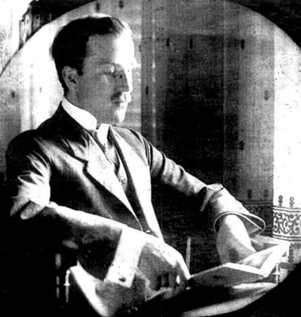
 Robert Lorenzini (pictured) adapted his master’s thesis on making purified steel to build a machine for pulling purified silicon for a semiconductor device startup.Photo: SEMI and Craig Addison/
The Chip Warriors
Robert Lorenzini (pictured) adapted his master’s thesis on making purified steel to build a machine for pulling purified silicon for a semiconductor device startup.Photo: SEMI and Craig Addison/
The Chip Warriors
David A. Stevenson, a newly arrived faculty member from MIT, challenged Lorenzini to tackle the problem of zone refining. Zone refining was a new technique developed by John Bernal and William Pfann to remove impurities from metals. It involves heating a narrow section of a crystal and then moving the molten zone along the length of the sample; impurities at the leading edge are moved to one end of the crystal, leaving behind a purer sample. As Lorenzini recalled in a later interview, Stevenson threw the idea in his lap and said, “Go design and build the equipment and see if you can do that.”
Pfann, a Bell Labs materials scientist, had applied the zone-refining process to germanium and silicon, but Lorenzini was working with stainless steel, for possible applications in aeronautics. The jet-engine industry had a problem with blade creep, caused in part by impurities in the steel that deformed the blades over time, eventually leading to engine failure. Lorenzini built a horizontal zone-refining apparatus for making purified steel and wrote his 1960 master’s thesis about it.
He was pleased to get an offer from Bethlehem Steel to join its management training program. But Leopoldo Valdes, who was known in the industry for his work on measuring the resistance of silicon and germanium using the four-point probe, persuaded Lorenzini to join the R&D staff at Rheem Semiconductor, a spinoff of Fairchild Semiconductor.
Jan Czochralski’s accidental discovery led him to develop a process for crystal growth
Rheem’s product line included diodes and transistors. Although the company could buy prepared silicon crystals, Valdes wanted to produce them in-house. He asked Lorenzini to design a machine to do that, applying what he knew about the zone refining of steel. It was Lorenzini’s first experience with silicon growing and “my first real assignment as an engineer,” he said in a later interview.
Lorenzini took his stainless-steel zone-refining machine, which had a horizontal orientation, and turned it vertical, the better to pull a uniform crystal of silicon from a molten lump of semiconductor. He designed the crystal puller on his own—no one else at Rheem was working on the process, and he had no other people in the industry to talk to about it.
 An accidental discovery in 1916 led the Polish chemist Jan Czochralski (pictured) to develop a method for pulling single crystals of semiconductors.Photo: The History Collection/Alamy
Lorenzini didn’t come up with the idea of pulling crystals. That process was discovered a half-century earlier by a Polish chemist named Jan Czochralski. According to some accounts, it happened by accident, while Czochralski was working one night in the metals laboratory of the engineering firm AEG in Berlin. Waiting for a crucible of molten tin to solidify, he absentmindedly dipped his pen nib into the metal instead of the inkpot. As he withdrew his pen, a long single thread of tin emerged. Eureka! Whether or not that story is true, Czochralski did write up his results for a German chemistry journal, and today he is credited with creating the crystal-pulling method that bears his name. In 2019, the Czochralski process became an IEEE Milestone.
A crystal puller has two main parts: a furnace and a puller. The furnace for Lorenzini’s first machine at Rheem consisted of a quartz crucible about the size of a thimble, to hold the silicon, and a radio frequency (RF) coil to heat the silicon to its melting point, approximately 1,440 °C. A small seed crystal was then introduced into the molten silicon, which would grow on the seed crystal as it was carefully pulled up with a smooth motion. After some trial and error, he got the machine working quite well.
The crystal then had to be thinly sliced into wafers and polished. Semiconductor devices are built on this silicon substrate. The wafers Lorenzini produced at Rheem were approximately 0.75 to 1 inch (22 to 25 millimeters) in diameter. Today, the industry standard is 300 mm.
Elmat’s first crystal pullers were built from salvaged parts
Lorenzini stayed at Rheem for two years before being lured away to become chief engineer at Allegheny Electronic Chemical Co. in northwest Pennsylvania. Allegheny had a large operation of about 20 crystal-growing furnaces and diamond-slicing saws, to produce silicon for the semiconductor industry. RCA was one of its biggest customers.
But Pennsylvania proved too snowy and cold for Lorenzini. After a year, he returned to California to work at Knapic Electro-Physics, which also manufactured silicon crystals. Dean Knapic, the founder of the company, was not one of the “traitorous eight” who defected from Shockley Semiconductor to found Fairchild, but he was a former Shockley employee—the industry was full of them at the time. Knapic was no longer at the company when Lorenzini arrived, and soon afterward, its financial backers decided to get out of the semiconductor business. They liquidated the company and auctioned off its equipment and materials.
 A single crystal of pure silicon like this will be sliced into wafers.Photo: Mark Williamson/Science Source
And so, in 1964, four years after graduating from Stanford and three jobs later, Lorenzini decided to go into business for himself. He bought motors, gear heads, and other spare parts from the Knapic auction and built his own larger, more efficient furnace, which became the cornerstone of his new company, Elmat. [The photo at top, from the collections of the Science History Institute in Philadelphia, shows one of the Elmat crystal pullers.]
Inspired by the quick changes executed by race car pit crews, Lorenzini designed his furnace so that workers could quickly take it apart, harvest the crystal, and reload it to start growing the next crystal. He knew that downtime meant lost profits.
Another innovation was the furnace’s heating element. Most furnaces were using RF to heat the crystal. In a break with tradition, Lorenzini switched to resistance heated furnaces, which worked by passing an electric current through a conductor to create heat and were less expensive to build.
By this point, Lorenzini was known for his expertise in crystal growing, and he had no trouble finding customers interested in buying Elmat’s silicon wafers. He started with Fairchild, RCA, and Texas Instruments. Later, IBM became Elmat’s biggest client. By 1968, the business was making around US $3 to 4 million per year when General Instruments purchased it.
Lorenzini took a year off before he founded his next company, Siltec Corp. Siltec pioneered zero-dislocation silicon, as well as the 3-inch (76-mm) wafer. Dislocations are irregularities in the crystal structure. Up until this point, silicon wafers could have thousands of dislocations per square centimeter of surface area. Siltec eliminated these dislocations by increasing the melt size of the crystal and introducing argon gas to flow through the chamber and cool the skin of the crystal. The ability to routinely produce zero-dislocation material was a game changer.
Lorenzini served as chairman and CEO of Siltec from 1969 to 1986. Two years after leaving the company, he cofounded SunPower Corp., which focused on low-cost, highly efficient solar cells. He has also been an angel investor in numerous startups.
In an interview in 2007, Lorenzini considered his career and realized there were a few critical decision points that could have set him on a very different course. He could have stuck with his original plan of studying mechanical engineering. Instead, he followed a charismatic professor into the field of metallurgy, which was undergoing its own transmutation into materials science. He could have accepted the generous job offer from Bethlehem Steel. Instead, he joined Rheem Semiconductor and the nascent semiconductor industry. Each step set him up for success as an entrepreneur who turned the tricky business of silicon-crystal growing from an art into a science.
Completing the history with a crystal puller’s perspective
This is not the article I planned to write when I first suggested crystal pulling to my editor. I wanted to focus on Jan Czochralski, but I could not find any historical artifacts linked to him. (The premise of this column is to use a museum object to tell an interesting history.) I even enlisted Janina Mazierska, the current chair of the IEEE History Committee. Her contacts in Poland came up with a lovely video (in Polish), but no suitable museum artifact.
The Elmat crystal puller at the Science History Institute (SHI) gave me a way to write about this history. But the narrative shifted away from Czochralski after I read the fabulous oral history interview with Lorenzini conducted by Hyungsub Choi, who happens to be one of my friends from graduate school.
Even then, my story felt incomplete. The curators at the Chemical Heritage Foundation (as the SHI was known at the time) had collected both a physical object and an interview with the object’s inventor, which meant they were choosing to preserve a particular slice of the history. Indeed, museums often focus on inventions and inventors to the exclusion of other narratives. Missing from the crystal-growing story was any information on what it was like to use one of these machines. Who were the workers who actually pulled the crystals?
It can be difficult to track down an invention’s users and convince them to share their experiences. By contrast, inventors can easily be traced through patent records, newspaper accounts, and the like. Rank-and-file workers typically don’t leave that kind of public record. Sometimes, though, museums get lucky.
 Patricia Anderson (left) operated the crystal pullers at Elmat in the late 1960s. On 20 June 1968, she managed the rare feat of extracting all of the molten silicon from the puller’s crucible, which she kept as a memento.Photos: Computer History Museum, Collection
102792161 and and
102806910
Patricia Anderson (left) operated the crystal pullers at Elmat in the late 1960s. On 20 June 1968, she managed the rare feat of extracting all of the molten silicon from the puller’s crucible, which she kept as a memento.Photos: Computer History Museum, Collection
102792161 and and
102806910
That’s what happened in February 2020, when Patricia Anderson contacted the Computer History Museum in Mountain View, Calif., and said she had a set of objects and documents from when she worked as a crystal puller at Elmat, Lorenzini’s company. Were the curators interested? Yes, they were!
As Anderson related in an oral history with David C. Brock, director of the museum’s Software History Center, a crystal puller like her would operate three to four machines at a time, constantly adjusting the temperature and pull rate to make sure the crystals were growing properly. Crystal pulling involved tacit knowledge—you had to develop a feel for how to adjust the machines. You couldn’t learn it from a book. On 20 June 1968, Anderson accomplished the rare feat of pulling a single crystal from all of the molten silicon in her crucible, a story she shared with Brock and that he included in a recent blog post.
Brock ends his post with a personal plea for more stories like Anderson’s, from those who worked in production and manufacturing in the electronics, semiconductor, and computing industries during the 1950s, ’60s, and ’70s. “The history of Silicon Valley is built from [these] stories,” Brock writes.
I will close with a similar request. I know that many people who read Past Forward are working engineers and technologists, and many of you have witnessed enormous transformations and fascinating events during the course of your career. If you want your experience to be part of the historical record, I urge you to sit down with an oral historian to document it or write up that account yourself.
For example, the IEEE History Center’s Mary Ann Hellrigel has been collecting oral histories from IEEE Life Fellows. I just started an oral history project on women working in the field of microwaves. If you don’t feel like talking to a historian, you can still share your experiences. Through the Engineering and Technology History Wiki, the IEEE History Center allows people to write up their own first-hand histories. Please consider contributing. Future historians will be grateful.
Part of a continuing serieslooking at photographs of historical artifacts that embrace the boundless potential of technology.
An abridged version of this article appears in the June 2021 print issue as “Crystal History.”
About the Author
Allison Marsh is an associate professor of history at the University of South Carolina and codirector of the university’s Ann Johnson Institute for Science, Technology & Society.