Scientists have been chasing silicon-based lasers for years—they’d provide a faster, cheaper way to move data across or between computer chips. Now researchers say they’ve gotten efficient light emission from silicon by forcing it into a new shape.
Replacing copper wires with beams of light makes it possible to send data from one transistor on a chip to another, or from one chip to another, at higher speeds and with less power, without having to worry about the excess heat generated by electrical resistance. Other types of lasers can do that, but the semiconductors they’re made of are more expensive than silicon, and they have to be manufactured separately and be attached to the chip. A silicon laser could be produced using the same processes for building the chips.
To reshape the crystal, the trick was to make it out of an alloy of silicon and germanium (SiGe), and grow it on top of thin nanowires made of gallium arsenide (GaAs). The GaAs crystal is naturally five-sided, so it forces the SiGe to take on the same hexagonal shape, even though a silicon crystal is normally a cube.
“We change the crystal symmetry and by doing this, we change the optoelectronic properties of the semiconductor,” says Erik Bakkers, head of the Advanced Nanomaterials and Devices group at Eindhoven University of Technology in the Netherlands. Bakkers and his colleagues published their work in the current issue of Nature.
Normally, silicon won’t lase because it has an indirect bandgap. In direct bandgap materials, when an excited electron drops from the higher-energy conduction band to the lower-energy valence band, it releases the excess energy as a photon. In an indirect-bandgap material such as silicon, excess energy comes out as heat instead of light. By reshaping the crystal, Bakkers and company essentially moved the bandgap to make it direct and allow the silicon to emit photons.
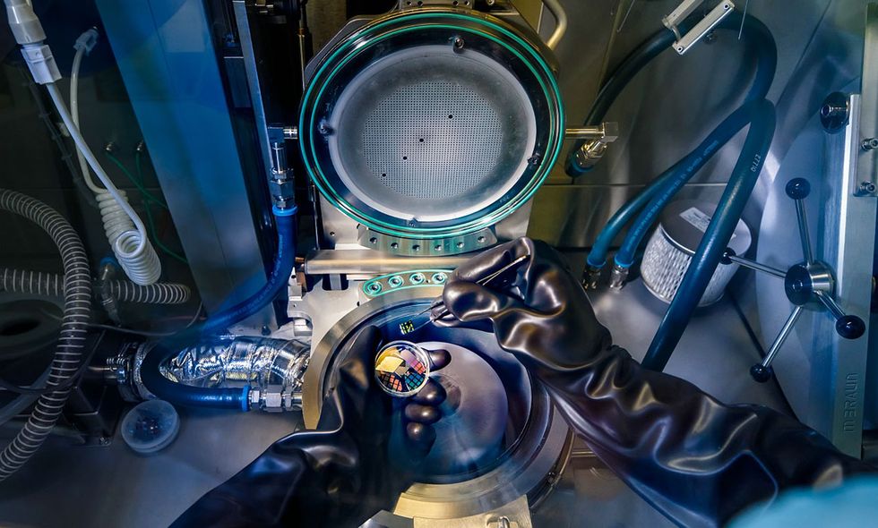 A look inside the Metal Organic Vapor Phase Epitaxy (MOVPE), which was used to grow nanowires with hexagonal silicon-germanium shells.Photo: Nando Harmsen/Eindhoven University of Technology
Though they were able to measure light emission, their material does not yet produce a laser beam. Bakkers is confident, though, that they’ll achieve that sometime this year. The germanium is also limiting them to producing light at a wavelength of 1800 nm. They’d like to get that to 1550 nm, the standard wavelength used in optical communications. They may be able to achieve that by introducing some mechanical strain on the silicon.
“The idea of exploring the hexagonal phase of SiGe for efficient light emission is interesting,” says Anthony Levi, a professor of electrical and computer engineering at the University of Southern California. He points out that there are a number of issues to be dealt with before this could be a practical silicon laser, including reducing defects in the crystal. Bakkers agrees there are challenges, but hopes to overcome them within the next four or five years.