The synergy of electronic processing and optical communications has powered the decades-long boom in information technology. But the need to convert signals back and forth between electrical and optical forms is becoming a bottleneck for the emerging field of integrated photonics.
A new type of switch that combines electrical and mechanical effects to redirect light could open the door to large-scale reconfigurable photonic networks for several applications including beam steering for lidars and optical neural networks for computing.
Currently, integrated photonics are used in high-performance fiber-optic systems , and a joint government-industry program called AIM Photonics is pushing their manufacture. However, current optical switches are too big and require too much power to blend well into integrated photonics. The new hybrid nano-opto-electro-mechanical switch has a footprint of 10 square micrometers and runs on only one volt—making it compatible with the CMOS (complementary metal-oxide-semiconductor) silicon electronics used in integrated photonics, says Christian Haffner from the Swiss Federal Institute of Technology in Zurich now working at the National Institute for Standards and Technology (NIST) in Gaithersburg, Maryland and the researcher who led the team that developed it.
The root of the problem Haffner set out to solve is that photons and electrons behave very differently.
Photons are great for communications because they travel at the speed of light and interact weakly with each other and matter, but they are much larger than chip features and require high voltages to redirect them because of their weak interactions.
Electrons are much smaller and interact much more strongly than photons, making them better for switching and for processing signals. However, electrons move slower than light, and more energy is needed to move them.
Long-distance communication systems process signals electronically and convert the signal into light for transmission, but converting between signal formats is cumbersome for local transmission. The new switch makes it possible to redirect optical signals on the integrated photonic circuit without having to convert them to electrical format and then back to optical format for further transmission.
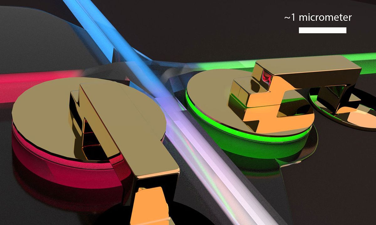
In Science, Haffner and colleagues describe a hybrid nano-opto-electro-mechanical switch that would occupy only about 10 square micrometers on an integrated photonic circuit. Their switch is a small multilayered disk sitting at a T-junction between two optical waveguides—stripes of transparent silica that guide light—that meet at a right angle. The top layer of the disk is a four-micrometer circle of 40-nanometer gold membrane resting on a small piece of alumina on layer of silicon deposited on silica. That structure acts as a curved waveguide resonant with both the input and output waveguides, so it can transfer resonant light between the two.
Light within the silica waveguides remains as photons, but within the switch the light excites oscillations of surface electrons in the gold, producing plasmons that vibrate at the frequency of the light wave but over a light much smaller than the optical wavelength. That tight confinement of the plasmonic part of the energy in the air gap between the gold and silicon creates a strong opto-electro-mechanical effect concentrated in the small volume of the switch.
With no voltage applied to the switch, the plasmonic waveguide remains resonant with the silica waveguides, so it couples light from the input waveguide to the output waveguide with minimal loss, as shown in the animation.
How the new nano-opto-electro-mechanical switch works.Video: NIST
Applying one volt to the switch produces a static charge that pulls the gold membrane toward the silicon layer, changing the shape of the waveguide in the switch so it shifts the phase of the light by 180 degrees. This causes destructive interference in the switch, breaking the resonance and the coupling of light into the side waveguide, so the light instead continues through the input waveguide to another switch.
"What we have in the end," says Haffner, "is a hybrid [switch], partly photonic and partly plasmonic, that manipulates light very efficiently." The plasmonic part concentrates the switching in a small area; the photonic part experiences low loss. Applying a one-volt bias compatible with CMOS electronics across such a short distance can produce a very strong force. That gives the switch a small footprint, low loss, and lower power consumption, which conventional electro-optic switches cannot achieve simultaneously.
Mass of the gold film is so low that the switch can operate millions of times a second. That's adequate for most switching, says Haffner, but it does have limits. The mechanical part of the switch cannot reach the picosecond speeds needed to modulate light in an optical transmitter.
The first applications are likely to be in laser beam steering for lidar, particularly for autonomous vehicles where continual information on the local environment is vital for safety. Another potential application is optical routing of signals on integrated photonic chips to create optical neural networks for deep-learning applications. The switch can redirect signals millions of times a second, a time scale needed by such applications.
"I don't see any issues in fabricating [the switches] with high yield," says Haffner.
Jeff Hecht writes about lasers, optics, fiber optics, electronics, and communications. Trained in engineering and a life senior member of IEEE, he enjoys figuring out how laser, optical, and electronic systems work and explaining their applications and challenges. At the moment, he’s exploring the challenges of integrating lidars, cameras, and other sensing systems with artificial intelligence in self-driving cars. He has chronicled the histories of laser weapons and fiber-optic communications and written tutorial books on lasers and fiber optics.


