For post-silicon electronics, engineers have been doubling down on research aimed at making transistors from atoms-thick two-dimensional materials. The most famous one is graphene, but experts believe that 2D semiconductors such as molybdenum disulfide and tungsten disulfide might be better suited for the job. Graphene lacks a bandgap, the property that makes a material a semiconductor.
Now, by combining graphene and MoS2, researchers have made a transistor that operates at half the voltage and has a higher current density than any state-of-the-art 2D transistor previously under development. This should slash the power consumption of integrated circuits based on these 2D devices.
“We were able to fully explore the untapped potential of 2D materials to make a transistor that shows better performance in terms of energy consumption and switching speed,” says Huamin Li, the electrical engineering professor at the University of Buffalo who presented the device at the IEEE International Electron Devices Meeting (IEDM).
Interestingly, the device takes advantage of graphene’s lack of a bandgap. In a transistor, a voltage at the gate electrode injects charge carriers into the channel region to create a conductive path between the source and drain electrodes. Conventional silicon transistors and 2D MoS2 transistors take advantage of the emission of high-energy “hot” electrons from the source. This places a fundamental limit of 60 millivolts for each ten-fold increase in the drain current (60 mV/decade).
But graphene, with no bandgap, acts as a “cold” electron source, Li says. That means less energy is required to send electrons out across the channel region to the drain electrode. The result: The device current can be switched on and off more rapidly.
“Using this unique mechanism we were able to break the fundamental limit of switching,” Li says. The group’s 1-nanometer-thick transistor needs only 29 mV to achieve that 10-fold change in device current. “We use less voltage to switch the device and control more current, so our transistor is much more energy efficient.”
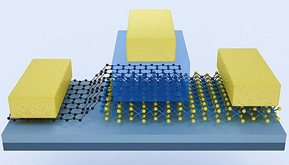
The researchers made the device by stacking a single sheet of graphene on a single layer of MoS2. This stacked region serves as the transistor channel, and the researchers deposit the gate electrode on top. The graphene monolayer acts as the source, while the molybdenum disulfide layer is the drain.
Other cold source materials such as 2D metals and electron-rich, n-doped semiconductors could also be used to break the 60 mV/decade limit, according to researchers from Shandong University who also presented their work at IEDM. Using simulations and modeling, they showed that n-doped graphene could bring the voltage down to 24 mV; even simply using n-doped silicon could bring it down to 33 mV.
Li says he and his colleagues chose MoS2 for their proof-of-concept device because it’s a 2D semiconductor that researchers have known and studied for a long time. Researchers from Taiwan Semiconductor Manufacturing Company also presented their latest findings on MoS2 transistors at IEDM.
These and other groups have not limited themselves to this 2D material. They are also working with materials such as tungsten disulfide (WS2) and black phosphorus. “If other materials work even better with our device technology, we will explore that,” says Buffalo’s Li.
Imec, in Leuven, Belgium, is placing its bets on WS2, which the company’s researchers believe should yield devices with the highest-ever performance. Two years ago, imec program director Iuliana Radu and her team developed a technique for placing a high-quality single layer of WS2 on a 300-mm silicon wafer. They now report that they can make WS2 transistors at wafer-scale. “The work paves the way towards industrial adoption of 2D materials,” they say.
Prachi Patel is a freelance journalist based in Pittsburgh. She writes about energy, biotechnology, materials science, nanotechnology, and computing.


