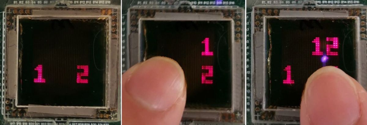
SuVolta's transistor design uses precision doping in order to lower power consumption and boost chip performance. When the company debuted, start-up executives pitched the approach as a simpler alternative to two other ways to improve transistor performance: moving to a 3-D structure, as Intel has and as the chip foundries are getting ready to, or building still-planar transistors on wafers that contain a thin layer of insulation. Those two techniques are often seen as rivals, although they can be used together (last year, for example, wafer manufacturer Soitec announced a new wafer line that it hopes will make it easier for chipmakers to adopt both).
While those alternate transistor designs are being adopted for the smallest transistors and most cutting-edge chips, SuVolta's first integrated circuit is squarely in the middle of the pack; it's made using a 55-nanometer manufacturing process, which is about six years behind today's most advanced 20- and 22-nm chips.
That's not a bad thing: many chips are still made using older manufacturing processes—more than half, according to the company’s press release—and there is likely a lot of value that can still be eked out of such technologies with optimization. But development is also afoot on the cutting-edge. When I spoke with Jeff Lewis, SuVolta’s senior vice president for business development and marketing, in July, he told me there is effort underway to apply the company's special sauce to more advanced chips. But he said the company is constrained from providing details by its partners, who ultimately decide if and how they discuss new products. "The majority of the company’s activity has actually been focused on 28 and 20, but we haven’t been able to talk about it," Lewis said.
Lewis said the company has six "engagements" with chipmakers, at manufacturing processes ranging from 65-nm to 20-nm. One is a recently announced partnership for 28-nm chips with Taiwan-based foundry UMC. Production of such chips won't start before 2015, according to an EETimes report. In the meantime, chipmakers are pushing their way down to 14 nm, with a variety of other technologies to assist them.
Image: SuVolta
Rachel Courtland, an unabashed astronomy aficionado, is a former senior associate editor at Spectrum. She now works in the editorial department at Nature. At Spectrum, she wrote about a variety of engineering efforts, including the quest for energy-producing fusion at the National Ignition Facility and the hunt for dark matter using an ultraquiet radio receiver. In 2014, she received a Neal Award for her feature on shrinking transistors and how the semiconductor industry talks about the challenge.


