A team of Japanese researchers has built the a new type of semiconductor that could drive down the lower limits on electronic component size and open up new avenues to fabricating low-power devices, persistent memories, and voltage-tunable optical switches.
Masayoshi Nakano and colleagues at RIKEN (in Osaka, Wako, and Tokyo) have demonstrated a novel Mott transistor based on vanadium dioxide. The device (described in "Collective bulk carrier delocalization driven by electrostatic surface charge accumulation" in the July 26 issue of Nature) exploits bulk changes in strongly correlated materials to produce potentially large amplification with low input power, and an unusual voltage-response profile.
Vanadium dioxide undergoes a first-order metal-insulator transition as temperature rises. The transition temperature varies depending on the strain in the VO2 layer and the direction of the transition: about 330 K to 340 K (57 C to 67 C) for a relaxed material and 280 K to 290 K (7 C to 17 C) for strained material. Above the transition temperature, vanadium dioxide behaves like a half-filled metal, the researchers note; at lower temperatures, its resistance jumps by “several orders of magnitude."
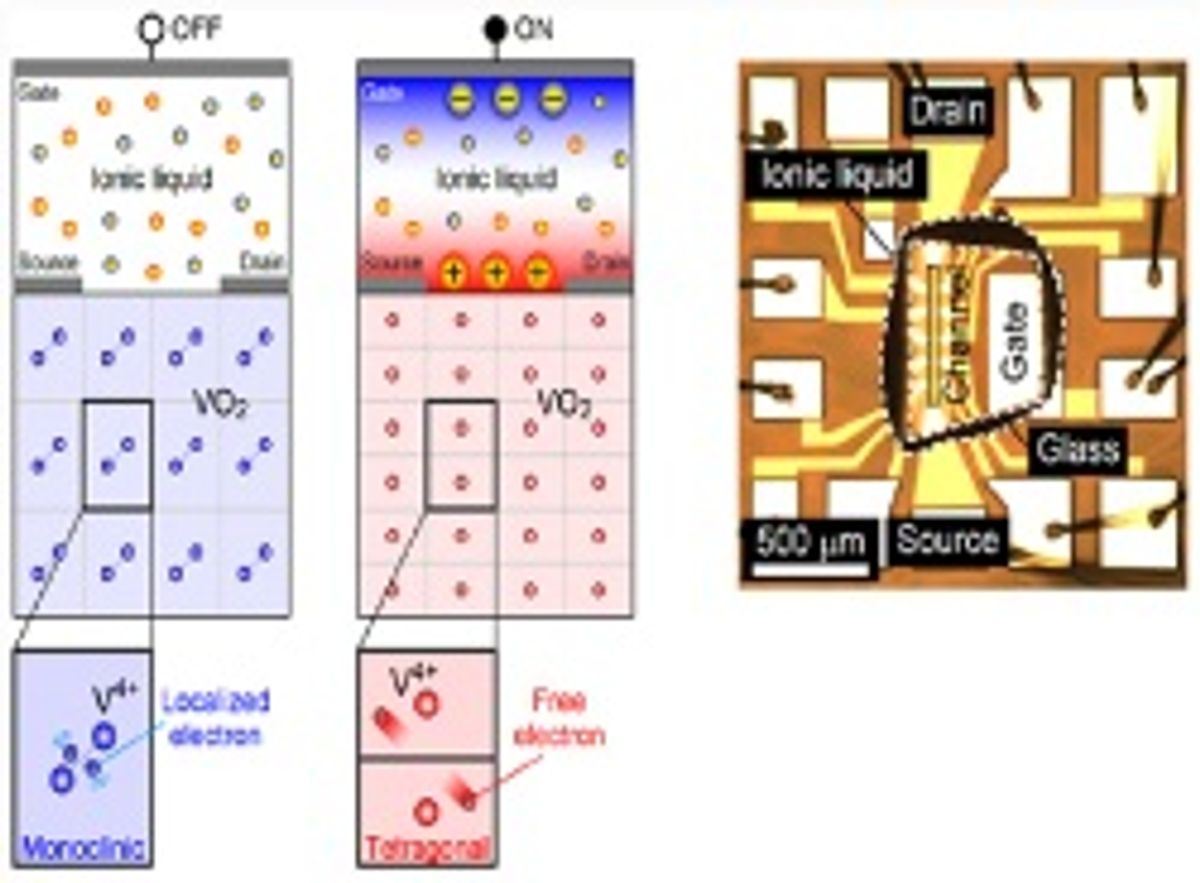
As its resistance alters, the material also appears to change its crystalline structure, shifting from monoclinic in the low-temperature insulator to a tetragonal lattice in the high-temperature conductor.
The researchers found that potential differences as low as 1 V could trigger durable shifts in resistance—“new behavior” beyond the reach of conventional metal-insulator-semiconductor field-effect transistors (MISFETs). A voltage-sweep experiment showed that resistance dropped by two orders of magnitude as voltages increased from +1 V to +3 V. The resistance remained low as voltage was then decreased, and remained steady as voltage dropped to zero and then reversed. Then, as the potential changed from about -2 V to -3 V, resistance sharply climbed again, by two orders of magnitude. The possibilities for non-volatile memory are particularly clear.
The RIKEN group made these electric-double-layer transistors (EDLTs) by depositing thin films of vanadium dioxide (tested in film thicknesses of 10, 20, and 70 nm) on a titanium dioxide substrate, with micro-deposited titanium-gold electrodes. The researchers coated the VO2 with an organic ionic liquid (N,N-diethyl-N-(2-methoxyethyl)-N-methylammonium bis-trifluoromethylsulphonyl)-imide, or DEME-TFSI for short). The ionic liquid is the key to allowing induced voltages to overcome Thomas-Fermi screening, a particular description of the electric field screening that damps the fields of moving electrons. This usually prevents induced fields from “penetrating” beyond 1 nm of the material's surface, inhibiting surface charge accumulation. Coating the vanadium dioxide layer with DEME-TFSI lets the charge accumulate, which in turn triggers the voltage-dependent bulk metal-insulator change similar to that induced by cycling the temperature.
Douglas McCormick is a freelance science writer and recovering entrepreneur. He has been chief editor of Nature Biotechnology, Pharmaceutical Technology, and Biotechniques.


