In September 2007, while leafing through his copy of IEEE Spectrum, Zhenqiang "Jack" Ma, an engineer at the University of Wisconsin-Madison whose research focus is microwave electronics, came across a news item that left him baffled: “I was shocked by the number of cell phones that are discarded daily in the U.S. and that are still in working order—426,000 per day. That is a huge number, and as a researcher, I was concerned,” he says. And rightly so; each cell phone contains chips made of poisonous gallium arsenide (GaAs).
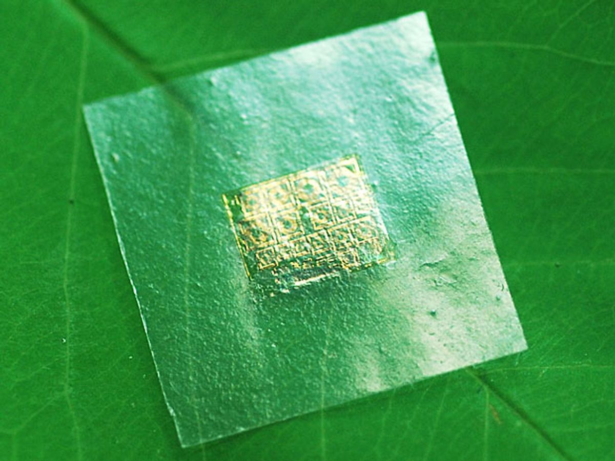
In the 26 May issue of Nature Communications, Ma and his colleague, materials scientist Shaoqin “Sarah” Gong, plus collaborators at UW-Madison and the Madison-based U.S. Dept. of Agriculture Forest Products Laboratory (FPL) published research describing a technique for making biodegradable semiconductor chips out of wood. What’s more, they demonstrated that microwave transmitter and receiver chips made this way perform as well as their silicon or GaAs counterparts. “Actually, our work was inspired by the IEEE Spectrum article,” says Ma.
Unlike the silicon, GaAS, and petroleum-based plastic substrates that are used in electronics—and are not biodgradable—the substrate for Ma and company’s "green" chips is made of a type of paper. But unlike paper, which typically consists of wood fibers 10 micrometers thick and bigger—making it rough and fairly easy to tear, they used much smaller fibers. “If you chop down the wood into nanosize fibers, you find that the fibers are single crystals. If you put this material together to make a substrate, it becomes very strong—stronger than the paper we use,” says Ma. “It also becomes transparent and has low RF energy loss," he adds. The cellulose nanofibril (CNF) “paper” they used is about 200 micrometers thick. Although the researchers coated it with a thin epoxy layer to protect it from moisture, this does not affect its biodegradability. "If we put it in a fungus environment, the fungus can still eat it," says the Wisconsin researcher.
To create the green chips, the researchers started out with silicon or GaAs devices sitting atop substrates made of the same material. Then they released the circuits from their original substrates and transfer-printed them onto the nanofibril substrates. Using this technique, the researchers created several microwave GaAs devices, such as arrays of GaInP/GaAs heterojunction bipolar transistors, as well as circuits containing capacitors, RF inductors and Schottky diodes. The performance of these flexible devices is exactly the same as that of rigid circuits, reports Ma.
The group also demonstrated several silicon-based digital logic circuits on paper substrates. However, these substrates may have a wider range of applications. Nanofibril films may be used in photovoltaic cells and also in displays because they have better light-transmission properties than glass, says Ma.
Using paper substrates would allow a reduction in the amount of GaAs used in chips by a factor of 3000, which would make chips conform to the pollution standards for arsenic set by the U.S. Environmental Protection Agency. Additionally, this technique would help cut costs, reducing the amount of expensive materials, such as gallium arsenide and highly purified silicon, that are packed into electronic gadgets.
"What we are looking at are future applications,” says Ma. The paper includes a market survey comparing today's production of rigid electronics with the projected flexible electronics production. The volume of flexible electronics is expected to largely exceed rigid electronics.


