The Conversation (0)

Practical Theorist: On 1 December 1957, physicist Jean Hoerni conceived the planar process, a technique used to manufacture essentially all silicon transistors and micro- chips today.
Photo: Hoerni: Wayne MIller/Magnum Photos; Photo-IllustratIon: Brandon Palacio
Not plastic bags, nor metal screws, nor cigarette butts. No, the commonest human artifact today is the transistor—invented 60 years ago this month by Bell Labs physicists John Bardeen and Walter Brattain. Millions of these subminiature switches populate computers, cellphones, toys, domestic appliances, and anything else that carries a microchip. Exactly how many transistors are around is hard to know, but several years ago Gordon Moore, a founder of Intel Corp. and author of the famed Moore’s Law, made an educated guess: more than 1018—that’s one quintillion—transistors are produced annually. “We make more transistors per year than the number of printed characters in all the newspapers, magazines, books, photocopies, and computer printouts,” Moore told me recently. “And we sell these transistors for less than the cost of a character in the Sunday New York Times.”
Behind the explosive growth that transistor production has seen since 1960 is a major technological achievement. Today, chipmakers essentially print transistors on silicon wafers. It’s a manufacturing method rooted in the mechanical printing process originated by Johannes Gutenberg more than 500 years ago—though far more complex, of course. Moore himself played a lead role in developing transistor-fabrication technology during the 1960s when he was research director at Fairchild Semiconductor Corp., in Palo Alto, Calif. But much of the credit for that revolutionary advance belongs to a lesser-known semiconductor pioneer and Fairchild cofounder. The unsung hero of this pivotal chapter in the history of electronics—the invention of the planar transistor—is Jean Hoerni.
A Swiss-born theoretical physicist, Hoerni, along with seven other determined, like-minded rebels—Moore, Robert Noyce, Jay Last, Sheldon Roberts, Eugene Kleiner, Julius Blank, and Victor Grinich—founded Fairchild in 1957 [see photo, "The Fairchild Eight"]. They all contributed, directly or indirectly, to the new technology, but none so much as Hoerni. Fifty years ago, sitting alone in his office, he elaborated a radically new kind of transistor: a more compact, flatter device whose sensitive parts were protected beneath a thin layer of silicon dioxide. Hoerni’s brilliant idea, more than any other single factor, allowed the fledgling firm to begin printing transistors on silicon. Planar transistors would prove to be much more reliable and perform far better than other designs, in effect rendering the competition’s offerings obsolete.
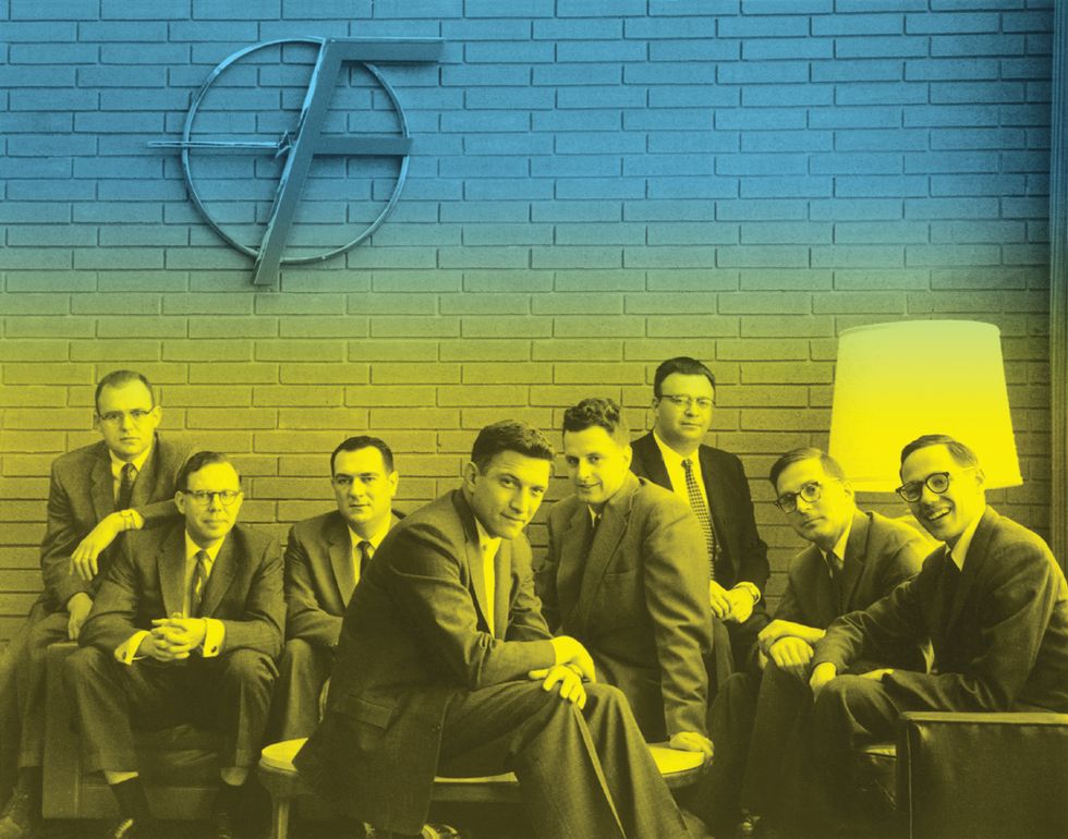 The Fairchild Eight: from left, Gordon Moore, Sheldon Roberts, Eugene Kleiner, Robert Noyce, Victor Grinich, Julius Blank, Jean Hoerni, and Jay Last.Photo-illustration: Wayne Miller/Magnum Photos/Fairchild Semiconductor
The planar process also made it easy to interconnect neighboring transistors on a wafer, paving the way to another Fairchild achievement: the first commercial integrated circuits. As other companies realized the great advantages of planar technology and began adopting it on their own production lines, Hoerni’s elegant idea helped to establish Silicon Valley as the microelectronics epicenter of the world.
The final months of 1957 were a time of anticipation at Fairchild as the founders organized the new firm’s labs and production lines in a group of buildings at 844 Charleston Road in Palo Alto. In September of that year, the eight scientists and engineers had resigned en masse from Shockley Semiconductor Laboratory, in Mountain View, about 2 kilometers away. They were rankled by the heavy-handed management style of its founder, transistor pioneer William Shockley, and his pursuit of difficult R&D projects at the expense of useful, salable products. So they persuaded the Fairchild Camera and Instrument Corp. of Syosset, N.Y., a firm looking to diversify its business, to found Fairchild Semiconductor. The eight founders planned to use the silicon processing techniques they’d learned under Shockley to make and sell advanced, high-speed transistors.
Their timing could not have been better. On 4 October 1957, the Soviet Union launched Sputnik I into orbit, igniting a frenzied space race with the United States. Millions worldwide gazed skyward to watch the awesome, undeniable evidence that the Soviets had a big head start. Meanwhile, Senator Lyndon B. Johnson (D-Texas) spearheaded congressional investigations into how the Eisenhower administration could ever have permitted such a “missile gap” to arise. With the USSR holding a major advantage in the greater thrust of its missiles, the U.S. aerospace industry sought every imaginable way to reduce the size and weight of its payloads and satellites. “There was a great deal of talk about the packing density of electronic functions in the late 1950s,” Noyce recalled in a 1975 interview, which is archived in the IEEE History Center. “It was the Missile Age, and transportation costs from here to Russia were very high.” The need for small, ultralight electronic circuits based on reliable silicon transistors made these devices a promising market for Fairchild.
That fall, the Fairchild founders worked feverishly to get everything up and running. Moore set up diffusion furnaces designed to impregnate silicon wafers with micrometers-thin layers of impurities—chemical elements such as boron, phosphorus, or aluminum that alter silicon’s electrical characteristics to form a transistor’s building blocks. Metallurgist Sheldon Roberts took on the task of growing high-purity silicon crystals from which the wafers could be sliced. Noyce and Last developed methods to do photolithography and oxide masking, by which they could define precise openings in a thin silicon-dioxide layer on the wafer surface; the impurities would diffuse through these openings into the underlying silicon. Other cofounders dug into manufacturing, testing, and selling the high-tech devices to aerospace customers.
And then there was Hoerni. A theorist with not one but two doctorates, from the Universities of Cambridge and Geneva, he had come to the United States to pursue postdoctoral studies at Caltech. In 1956, Shockley lured the 32-year-old physicist away from academia and assigned him to do theoretical calculations of diffusion rates. At first, Hoerni was cloistered in a separate office, but he kept coming around and snooping in the lab in the main building—which gave him valuable insights into solid-state diffusion. Later, at Fairchild, while the others worked on building or installing equipment, he mostly sat in his office and ”scribbled in his notebook,” Moore told me.
On 1 December 1957, Hoerni grabbed his crisp new lab notebook and began writing an entry titled “Method of protecting exposed p-n junctions at the surface of silicon transistors by oxide masking techniques.” In a loose, fluid scrawl interspersed with three simple drawings, he described a revolutionary new way to fabricate transistors—unlike anything ever before attempted.
The most advanced silicon transistors at that time were called mesa transistors because they resembled the plateaus of the American Southwest, the impurity layers running laterally like the colorful rock strata [see illustration, "Mesa vs. Planar"]. These transistors basically consisted of three impurity layers piled up vertically, each rich in either electrons (n-type) or electron deficiencies, better known as holes (p-type). The main drawback of the mesa structure is that its p-n junctions, the interfaces between layers where the transistor’s electrical activity occurs, are exposed at the edges. Bits of dust or drops of moisture can contaminate the sensitive interfaces and disrupt their normal electrical behavior.
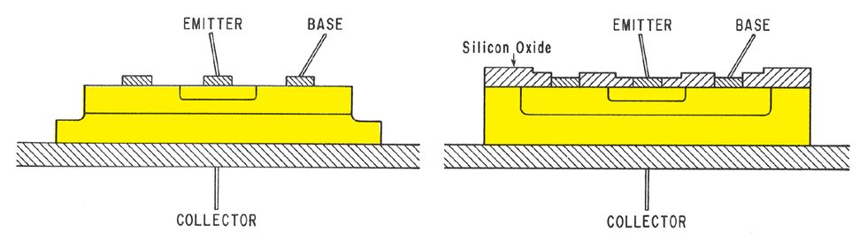 Mesa vs. Planar: Side views of a mesa (left) and a planar transistor, from a report Hoerni prepared in 1960.Illustration: Computer History Museum
Hoerni’s idea was to protect the p-n junctions by keeping the oxide layer in place upon the silicon after the diffusion process; the standard practice at the time was to etch that layer away, baring the junctions. “The oxide layer so obtained is an integrant [sic] part of the device,” he wrote in his notebook that December day, “and will protect the otherwise exposed junctions from contamination and possible electrical leakage due to subsequent handling, cleaning, and canning of the device.”
It was a brilliant conception but too far ahead of its time. Hoerni’s approach would require additional fabrication steps, and making mesa transistors was already at the limits of the possible. Bell Labs and Western Electric had produced prototypes of mesas, but no company had sold one on the open market.
In early 1958, Fairchild secured its first purchase order for silicon transistors from IBM’s Federal Systems Division, which planned to use them in the onboard computer it was designing for the B-70 bomber. Fairchild, which didn’t even have prototypes, faced the formidable challenge of delivering real working devices. To maximize the chances of success, the cofounders decided to develop two different kinds of mesa transistors. A group under Moore pursued the n-p-n transistors, which were thought to be easier to fabricate, while Hoerni formed another group to delve into the p-n-p versions.
Crucial to both efforts was the work Last and Noyce were doing on the optical methods needed to transfer the patterns defining a transistor’s features onto the silicon wafer. On a trip to San Francisco, they purchased three 16-millimeter lenses from a camera store and used them to fashion a step-and-repeat camera, a contraption that produced rectangular arrays of tiny, identical images on photographic plates, called masks. Workers shone light through the masks onto a special photosensitive resin that had been deposited on the wafer’s oxide surface layer. When they subsequently rinsed the wafer in a powerful acid, it etched the illuminated areas away, exposing the silicon beneath them. Thin layers of impurities were then diffused into the silicon through the resulting openings. Using such techniques, Fairchild could batch-process hundreds of identical transistors on a single wafer.
Another breakthrough was the use of a single metal to make the electrical connections to both n-type and p-type silicon, an approach that greatly simplified the manufacturing process. Moore had been struggling with this issue, trying many different metals, when Noyce happened by his lab early one day and suggested aluminum. As a p-type impurity, aluminum easily bonds to p-type silicon but often sets up a current-blocking p-n junction when it is deposited on n-type silicon. Moore found a way around this problem by starting with n-type silicon that had more impurities than usual. Moore’s group got its n-p-n transistors into production in May 1958, well ahead of Hoerni’s team, which had opted to use silver for electrical contacts.
To protect the mesa’s sensitive junctions, each transistor was packaged into a pea-size hermetically sealed metal can and then tested. Fairchild shipped the first hundred of them to IBM on schedule that July, billed at US $150 apiece. The next month, at the WESCON electronics trade show, the founders discovered to their delight that they were the only ones with silicon mesa transistors on the market. “We scooped the industry!” Noyce said, exulting at a Fairchild meeting a few days later.
About the only person at Fairchild not celebrating was Hoerni. A proud, charming, but irascible and often volatile man, the scion of a Swiss banking family, he was miffed that his p-n-p approach had been passed over. But he was also a hardheaded contrarian whose creative fires were stoked by adversity. Hoerni not only didn’t give up, he set out to develop an even better transistor. Later that year, he returned to the ideas written down in the opening pages of his notebook. Could the oxide layer in fact be used to protect the sensitive p-n junctions? There were indications it might. That spring, reports had come in from Bell Labs that the oxide layer indeed protected the silicon underneath. Why not the junctions, too?
With a doctorate in crystal physics, Hoerni realized that the impurity atoms coming through the tiny openings in the oxide layer would diffuse sideways nearly as well as downward into silicon’s crystal structure. Which meant that the junction interfaces would curl up under the oxide layer surrounding an opening, just micrometers farther out from its edges. If left in place instead of being etched away, he figured, the oxide layer could protect those junctions.
But the device Hoerni envisioned would not only be more difficult to fabricate, its structure flew in the face of conventional wisdom. Especially at Bell Labs and Western Electric, the oxide layer was considered ”dirty”—filled with impurities after the diffusion process—and thus had to be removed.
Meanwhile, serious concerns began to emerge in late 1958 and early 1959 about the mesa transistors Fairchild was selling. Some of the devices were experiencing amplification instabilities, and others were malfunctioning. One important customer reported that a transistor had suddenly stopped working altogether. A Fairchild technician eventually traced the failures to tiny dust particles and solder fragments trapped inside the cans. The specks were attracted to the junctions by the strong electric fields there. In a subsequent quality-control procedure that became known as the tap test, workers would tap on the cans with pencil erasers, trying to dislodge any bits that might short out the junctions. If that happened, the transistor was discarded. Those were anxious days for the brash young firm, for such failures in its only product threatened its very existence.
Hoerni’s single-minded pursuit of a more reliable transistor proved timely indeed. In what Moore described to me as a “kludge experiment” intended to assess Hoerni’s ideas, a technician deliberately left the oxide layer on top of one of the p-n junctions in a mesa transistor. When tested, it had substantially better amplification stability—suggesting that Hoerni was truly onto something. On 14 January 1959, he had two of his notebook pages typed up as a formal disclosure and sent to John Ralls, Fairchild’s patent attorney. Other than a few minor corrections and better drawings, it was identical to the notebook entry he had written more than a year earlier.
One problem with Hoerni’s approach—and part of the reason nobody attempted it at first—was that his transistor structure was more complex than the mesa’s, requiring a fourth photolithographic mask to fabricate it. Last and Noyce’s step-and-repeat camera could accommodate only three masks. But that February, Last “jury-rigged a fourth mask” for this purpose, he recalled in a recent telephone interview. On 2 March, Hoerni wrote another entry in his notebook titled “A method of manufacture of PNP transistors with oxide protected junctions.” In two more pages of text and drawings, he indicated specifically how to fabricate such a device, though still stubbornly using silver for the electrical contacts on the top side. By then, his technicians were already transforming his novel ideas into actual fabrication processes.
But all that progress came at a time of upheaval at Fairchild. The same week that Hoerni was jotting down his fabrication ideas, Edward Baldwin, who had been hired from Hughes Electronics Corp. to serve as Fairchild’s general manager, departed abruptly to found Rheem Semiconductor in Mountain View, taking with him five key people from the manufacturing division. After persistent urging by the other Fairchild cofounders, Noyce stepped up to replace him, and Moore took over Noyce’s position as research director.
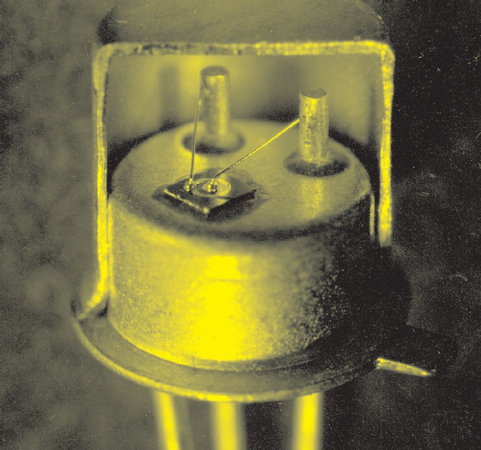
 Silicon Flatland: Above from top, an early prototype planar transistor made by fairchild in the spring of 1959; a cutaway model of the company’s first commercial planar transistor, the 2n1613, initially marketed in April 1960; one of the first integrated circuits made by Jay Last’s development team in the spring of 1960; and a prototype planar flip-flop circuit fabricated in the fall of 1960.Photos: Top (2): Fritz Goro/Time & Life Pictures/Getty Images; Bottom (2): Fairchild Semiconductor
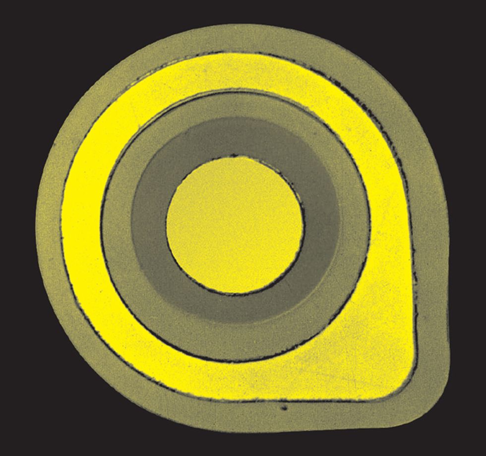
The following week, Hoerni invited several colleagues to watch a demonstration of his new prototype transistor. Under a microscope it appeared unlike any other Fairchild device. Less than a millimeter across, it was completely flat—no mesa protruded in the middle. All that was visible was a circular metallic dot with a metal ring around it, plus the oxide surface layer between them. It resembled a bull’s-eye target with a portion of it pulled out like a teardrop, making it easier to attach a wire [see photos, "Silicon Flatland"].
What happened next is unclear. Some observers have claimed that Hoerni suddenly spat on his transistor, to demonstrate that such outrageous abuse had no ill effects on the oxide-protected junctions. But Last and Moore don’t recall him actually spitting, and Moore points out that saliva would have shorted out the metal wires on the device. Even so, the demonstration was dramatic and convincing, Last told me. “Gee, it’s too bad Baldwin had to leave last week,” he recalls joking afterward.
Things moved swiftly after that. It was obvious that Hoerni’s creation was far more rugged and reliable than the mesas. And it also proved to have much lower leakage currents—small, wrong-way trickles that can seriously degrade transistor performance. In a Fairchild report released the following year, Hoerni observed that the leakage currents in his device were usually less than a nanoampere, or as little as 1 percent of those in mesa transistors.
The nagging question on everyone’s mind was, Can we manufacture these transistors in quantity? Initially, the planar process yielded only a few working transistors in every 100—much worse than the mesa process. But as various problems, such as pinholes in the oxide layer, were resolved, yields rose and doubts evaporated. In April 1960, Fairchild sold its first planar transistor, the 2N1613—a metal cylinder about half a centimeter in diameter and almost as high, with three little metal legs sticking out beneath it.
A few months later, Noyce and Moore decreed that henceforth all the company’s transistors would be planar. While other semiconductor firms such as Rheem, Motorola, and Texas Instruments had begun churning out competitively priced mesa transistors, Fairchild boldly struck out in a promising new direction. Soon avionics manufacturers began to demand planar transistors because of their unmatched reliability. The Autonetics division of North American Aviation, for example, insisted on using Fairchild’s planar transistors in the guidance and control systems for the Minuteman missile.
Fairchild eventually licensed the planar process to other transistor makers—even Bell Labs and Western Electric. Either the other firms followed Fairchild’s lead or they exited the industry.
Well before Fairchild succeeded in commercializing Hoerni’s device, Noyce had begun thinking about what else the company could do with the planar approach. In his 1975 interview, he credited patent attorney Ralls with challenging the Fairchild team to consider other applications that could arise from the new way of making transistors. Noyce realized that by leaving the oxide layer in place, “the surface of the silicon then had one of the best insulators known to man covering it.” Which meant that the electrical connections could be made by depositing strips of metal—such as the aluminum contacts Moore’s group had perfected—on top of the oxide layer. The strips would be automatically insulated from the components underneath.
On 23 January 1959, not long after Hoerni had his patent disclosure typed up, Noyce penned an entry in his own notebook: “In many applications now it would be desirable to make multiple devices on a single piece of silicon in order to be able to make interconnections between devices as part of the manufacturing process, and thus reduce size, weight, etc., as well as cost per active element.” His entry went on for another four pages and included the crucial idea of using the oxide layer as an insulator underneath the connections. He also described a way to isolate the circuit elements—not just transistors but also resistors, capacitors, and diodes—from one another by inserting between them extra p- junctions, which permit current flow in only one direction.
Did Noyce recognize the significance of these ideas at first? In those days, researchers at Bell Labs, Fairchild, and elsewhere often had a colleague immediately witness and sign important, potentially patentable ideas. Noyce, for instance, had witnessed Hoerni’s entry back in December 1957. Curiously, however, nobody witnessed Noyce’s entry, suggesting that he did not consider it all that important when he wrote it.
Around that time, the “monolithic idea” of fabricating complete, rugged electronic circuits in a single chunk of silicon, germanium, or other semiconductor was becoming fashionable. The U.S. Army, Navy, and Air Force were each promoting their own pet approaches and funding R&D contracts in industry. Monolithic integration was considered a way to overcome the “tyranny of numbers” bemoaned by Bell Labs Vice President Jack Morton. He had warned that as the number of circuit components increased, so did the likelihood of circuit failure [see “How Bell Labs Missed the Microchip” IEEE Spectrum, December 2006]. But what if you fabricated reliable components and interconnected them in a single semiconductor chip? Then your odds of building successful complex circuits might be much higher.
In August 1958, Jack Kilby at Texas Instruments had conceived a way to make such integrated circuits in silicon. He even built a prototype oscillator based on the idea, using germanium mesa transistors, which were then readily available at TI. But while Noyce’s subsequent approach involved metal strips deposited on an oxide layer, Kilby’s device used “flying wires” to make the electrical connections. TI publicly announced this breakthrough on 6 March 1959 at a gathering of the Institute of Radio Engineers (a predecessor of the IEEE) in New York City. TI President Mark Shepherd boasted that it was “the most significant development by Texas Instruments since we divulged the commercial availability of the silicon transistor.”
News of TI’s achievement reached Fairchild just as its management turmoil was winding down and Hoerni was about to demonstrate his new transistor. Later that month, Noyce called a meeting to discuss how to respond to TI and revealed his thoughts about how to interconnect multiple devices in silicon. By then it was becoming obvious that Hoerni’s planar process offered major advantages in fashioning such integrated circuits. Hoerni, Last, Moore, and the other cofounders discussed that possibility extensively, with the emphasis on the pragmatic. “Any one of us could think of ten things we might do, but then we’d rule out nine or even ten of them as impractical,” Last said in a recent phone conversation. “We were focused on making things that worked.”
Out of this creative stew emerged another crucial concept, which historians have so far overlooked. With the planar transistor, it was now easy to put all three electrical contacts—to the emitter, base, and collector—on one side of the silicon wafer. At first glance, it might seem just a marginal improvement, but this feature, plus the fact that a single metal such as aluminum could be used to form the connections, meant that Fairchild could now, in effect, print electrical circuits—transistors and all—on silicon. Like the typographic patterns of ink impressed onto paper by a printing press, the patterns of the individual semiconductor devices and metal interconnections could now be imposed photolithographically on a single side of a wafer.
Hoerni was the first to publish the concept of putting all the electrical contacts on one side. In his patent application for a “Method of Manufacturing Semiconductor Devices,” filed on 1 May 1959, he presented the idea almost as an aside, after revealing a structure closer to that of the mesa, with contacts on both sides of the wafer. In Noyce’s much more famous patent, “Semiconductor Device and Lead Structure,” filed three months later, the single-side feature is a fundamental aspect of his planar integrated-circuit structure. But neither man’s lab notebook mentions the idea—suggesting that it probably emerged from the fertile give-and-take discussions that spring and was later added to the patent applications.
In any event, that special feature of the planar process gave Fairchild a tremendous advantage in realizing the monolithic idea.
To implement this new technology, Last formed a group in the fall of 1959, aiming to manufacture integrated circuits based on Hoerni’s planar process. It took another 18 months before the first commercial microchips, Fairchild’s Micrologic series, reached the market. But Fairchild still came out with its microchip more than six months ahead of TI, which succeeded only after it began using the planar technology it had licensed from Fairchild.
To achieve this goal, Last’s team had to overcome several significant obstacles. Tolerances were a lot tighter on positioning the physical features of these chips—which meant the various masks had to be aligned more precisely. Finding a way to isolate their components electrically was also a thorny problem. Noyce’s idea of inserting back-to-back p-n junctions between individual components proved an effective solution, opening the door to commercialization in March 1961.
But Hoerni and Last were not around to share in the celebrations. They had become disenchanted with the increasingly stratified Fairchild hierarchy and the worsening relations with its New York parent. They also felt that Fairchild’s marketing department opposed microchips because they’d compete directly with the company’s principal products—transistors and diodes. So Hoerni and Last departed to start yet another semiconductor operation, the Amelco division of Teledyne, with the goal of producing integrated circuits.
Close friends since their days at Shockley Lab, the two often spent their weekends together hiking in the deserts and mountains of the Southwest. Last remembers that Hoerni had incredible stamina and could hike for hours on little food or water. To lighten his load, he carried only a skimpy old sleeping bag. When temperatures got too cold, he’d stuff it with newspapers—once claiming that The Wall Street Journal provided the most extra warmth.
In two years, however, Hoerni began to have problems with the new company. In the midst of a cash crunch in April 1963, Teledyne executives suggested that he be reassigned from general manager of Amelco to director of research as a cost-cutting measure. The moody Swiss physicist did not warm to the idea. Instead, he decided to leave the firm and began casting around for other business alternatives.
Although their relationship was “rather frosty” after Hoerni’s decision, Last says, they still headed out that spring for a 3000-meter climb in the Inyo Mountains east of the Sierra Nevadas. Exhausted, they reached the summit at dusk, just before a cold front pushed through and temperatures plummeted. Despite their differences, the two huddled together the rest of the night to keep from freezing. “We climbed down the next morning, drove back to the Bay Area, and continued our frosty business discussions,” Last recalled years later, during a memorial service for his friend.
While Last remained with Teledyne until the late 1970s, Hoerni went to work for Union Carbide, setting up its semiconductor division. In 1967 he ventured out in yet another direction, founding Intersil Corp., with European investors, to make microchips for digital watches; it was the first company to produce such low-voltage, low-power circuits based on CMOS (complementary metal-oxide-semiconductor) technology. The following year Moore and Noyce abandoned Fairchild to launch Intel in Santa Clara, Calif., at the heart of what soon became known as Silicon Valley.
For the next three decades, Hoerni remained active as an investor and consultant in the semiconductor industry. He also became involved in philanthropic initiatives and continued trekking throughout the world. He died in Seattle on 12 January 1997, the year the transistor turned 50. Although often overlooked in semiconductor history, he should be remembered as the person who engineered the all-important bridge from this revolutionary solid-state device to the integrated circuit, which has become so ubiquitous today.
About the Author
Contributing Editor Michael Riordan teaches the history of physics and technology at Stanford University and the University of California, Santa Cruz.
To Probe Further
For excellent accounts of the early Fairchild work and its wider implications, see Gordon Moore’s “The Role of Fairchild in Silicon Technology in the Early Days of ’Silicon Valley’ ” and Jay Last’s “Two Communications Revolutions,” both in Proceedings of the IEEE, Vol. 86, No. 1 (January 1998).
Two recent books that go into great detail about planar technology and the origins of the silicon integrated circuit are Christophe Lécuyer’s Making Silicon Valley: Innovation and the Growth of High Tech, 1930–1970 (MIT Press, 2006) and Leslie Berlin’s The Man Behind the Microchip: Robert Noyce and the Invention of Silicon Valley (Oxford University Press, 2005). A review of both books appeared in the April 2006 issue of IEEE Spectrum.
The Computer History Museum explores semiconductor history at https://www.computerhistory.org/semiconductor.


