The Conversation (0)

Photo: Intel
Moore’s Law has been called the greatest winning streak in industrial history. Here we look back at some of the key milestones, developments, and turning points that have kept the streak alive for a half century.
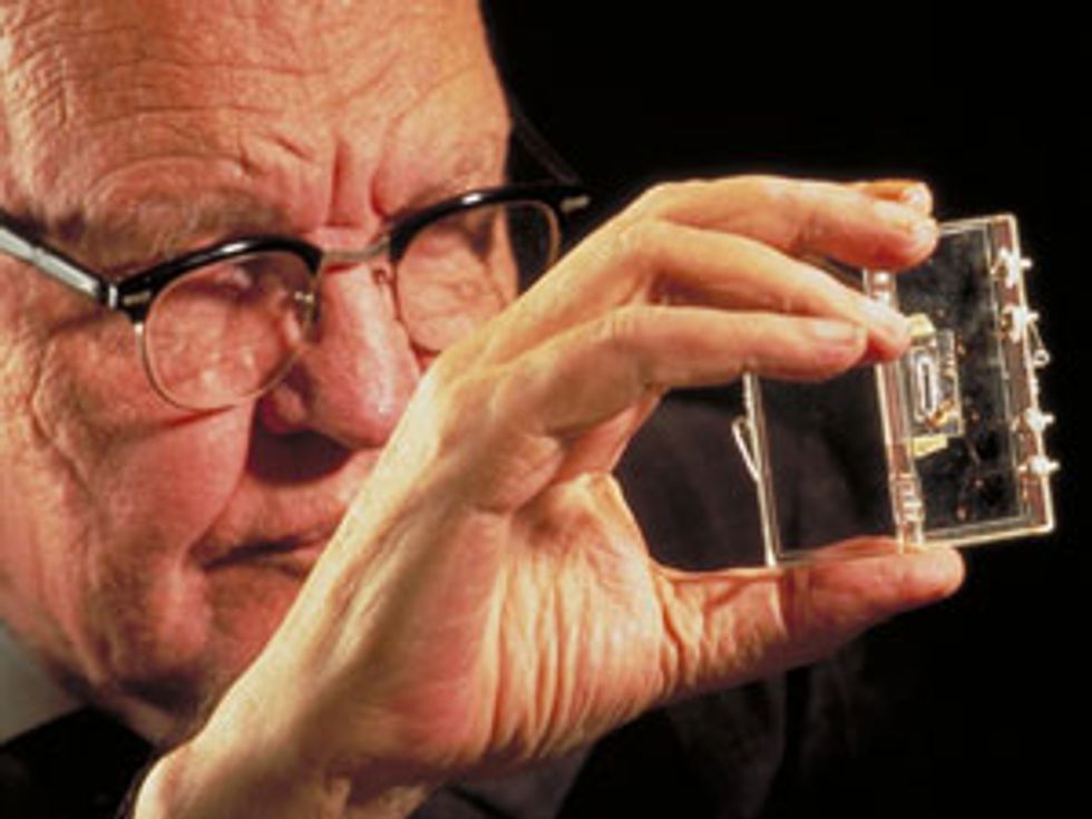 Photo: Texas Instruments
September 1958
Jack St. Clair Kilby tests the world’s first integrated circuit. The single-transistor oscillator is built on a chip of germanium in a lab at Texas Instruments.
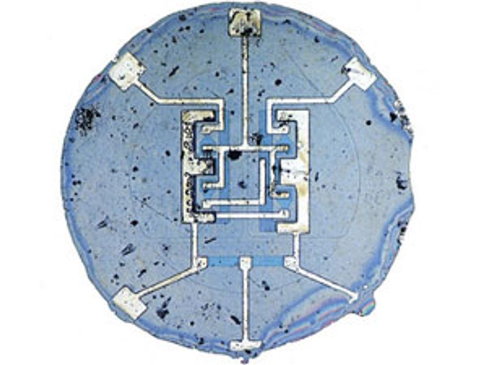 Photo: Fairchild Semiconductor
March 1959
Jean Hoerni of Fairchild Semiconductor Corp. demonstrates his planar process, which produces flat, reliable transistors suitable for inclusion on chips. It later prompts Moore to write that “the available data I chose (for the Electronics magazine article) started with the first planar transistor, which had been introduced in 1959.” Building on Hoerni’s invention, Robert Noyce, a colleague of Hoerni’s at Fairchild Semiconductor, conceives and documents a method of producing integrated circuits based on Hoerni’s planar components. In August 1959, Noyce puts coworker Jay Last in charge of a group at Fairchild to make planar integrated circuits. The group produces its first circuit in May 1960. After patent disputes and debates in the 1960s and 1970s, the technology community settles on the idea that both Kilby and Noyce are the separate inventors of the integrated circuit.
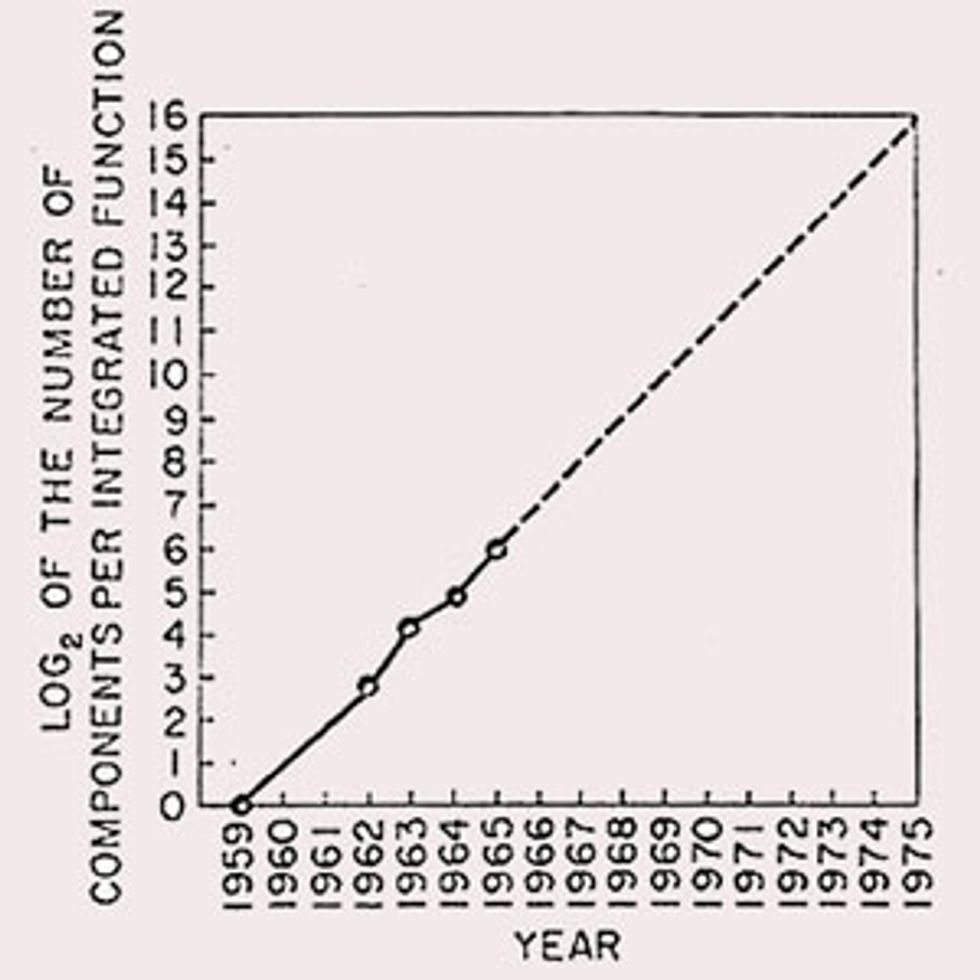 Image: Intel
April 1965
Gordon Moore’s famous article is published in Electronics magazine. In the article, Moore predicts an annual doubling of component density on an integrated circuit at minimum manufacturing costs. Moore later identified “a component” as “transistor, resistor, diode or capacitor.” The 1965 article follows the pioneering work on integrated circuits, started in 1958, by Jack Kilby at Texas Instruments and Bob Noyce and others at Fairchild.
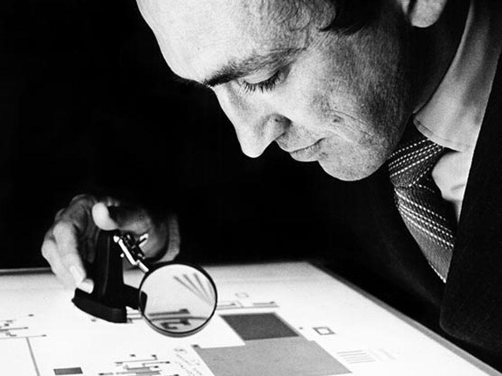 Photo: IBM
Autumn 1966
IBM researcher Robert H.
Dennard hears a presentation by coworkers trying to improve magnetic core memory. That night, on his couch at home, he thinks, “What could I do that would be really simple?” Thinking of MOS technology, he realizes that a stored charge on a capacitor could represent a bit of information, while a transistor could control the writing of that charge. Shortly after, he proposes the single transistor/single capacitor (1T/1C) dynamic RAM, which eventually gives rise to a vast new industry.
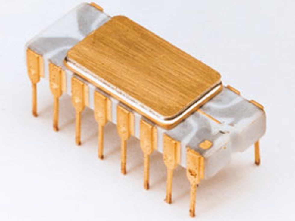 Photo: Intel
April 1970
Design begins on the world’s first general-purpose programmable microprocessor, the Intel 4004. Demand for ever more integrated chipsets, driven by the portable calculator industry, spurs Intel, Mostek, Texas Instruments, and others to develop new calculator ICs. The 4004, supplied to Japanese calculator maker
Nippon Calculating Machine Corp., runs at 108 kilohertz, has 2,250 transistors, and is created in 10-micrometer technology on 2-inch wafers.
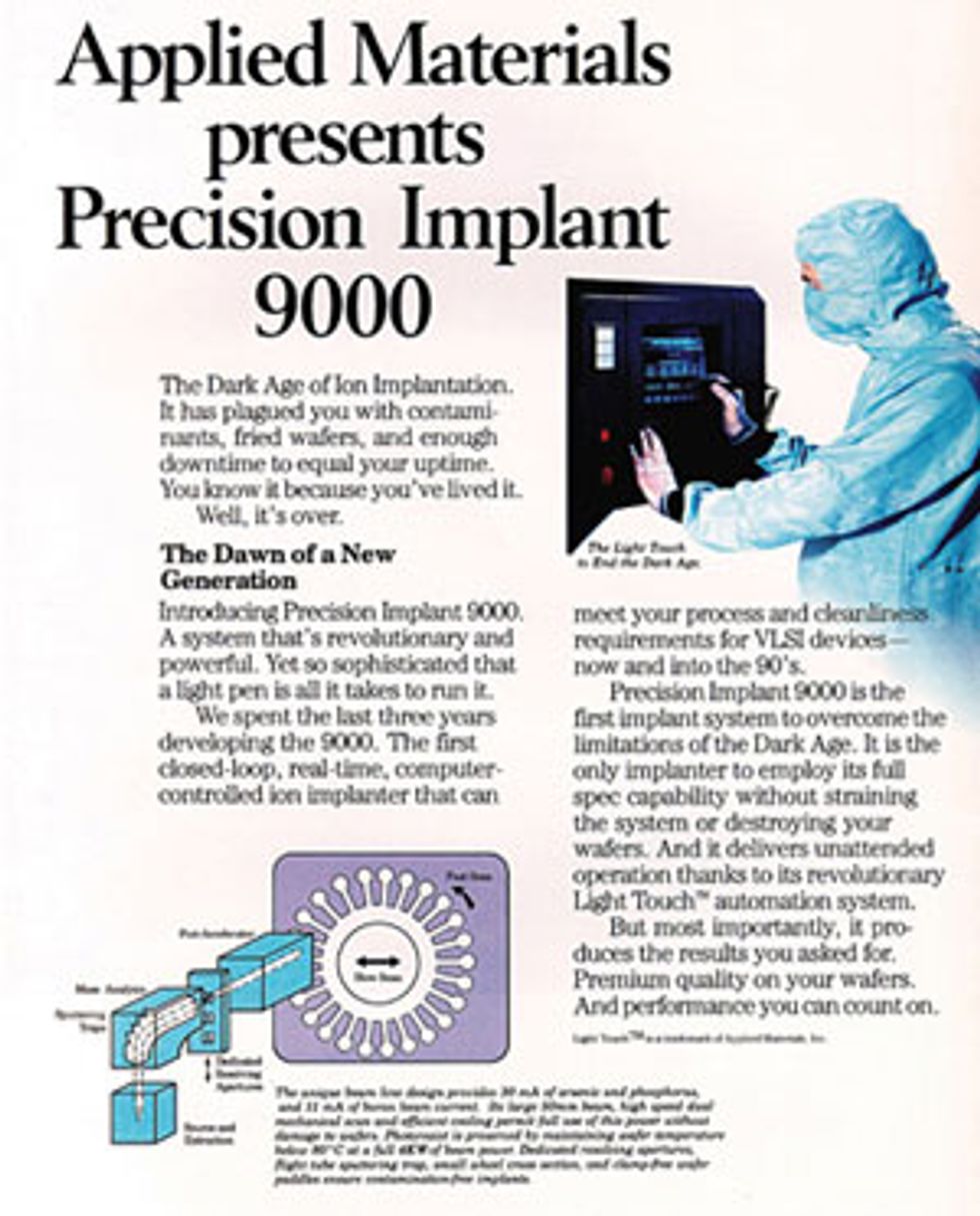 Photo: Applied Materials
June 1972
Semiconductor makers begin switching from one doping method to another. With
doping, atoms of an element are forced into a semiconductor crystal to change its electronic properties. The new doping method, called ion implantation, involves high-energy bursts of dopant ions including boron, phosphorus, and arsenic. The older method, called blanket diffusion, introduced dopants using doped glass and furnaces.
1973
Perkin-Elmer’s Micralign projection scanner is introduced. It kicks off an evolution in
lithography from contact printing to optical projection. The Micralign system uses a lens to project onto the wafer, at 1:1 scale, an image of the pattern on the mask. The mask is a sort of stencil to make a layer of a chip. The projection scanner is followed five years later by the stepper, which repeatedly projects mask images onto the wafer, one after another. Nikon’s NSR-1010i3 stepper with a 365-nanometer wavelength, based on an i-line light source, ships in 1984. The first deep ultraviolet (DUV) stepper, with a 248-nm-wavelength light source, ships from the GCA Corp., beginning the era of reduction printing, in which the image on the mask is larger than what is printed on the wafer. Moore, in 1995, credits “moving to optical projection rather than contact printing of the patterns on the wafers” as a key contributor to scaling in the early years of the industry.
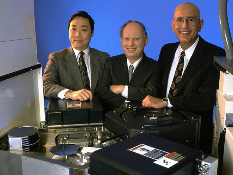 Photo: Applied Materials
March 1974
U.S. and Japanese chipmakers begin adopting techniques to
etch their wafers with “dry” methods based on the use of a plasma, an improvement on the wet methods based on chemicals. These etch steps, along with the deposition ones that precede them, are the core of transistor fabrication. The move to dry etching is necessary because the insulating films, such as silicon dioxide and silicon nitride, are becoming so thin that they cannot be readily etched by the traditional, wet processes. The switch to these plasma-enhanced etching techniques brings a fundamental change to chip fabrication because they require that single wafers be processed in a chamber; with the wet process, multiple wafers were bathed simultaneously in chemicals. In the early 1980s, Bell Labs researchers, including Dan Maydan, David N.K. Wang, and Sass Somekh [above], are recruited to join Applied Materials, then a relatively small maker of chip fabrication equipment, to commercialize plasma-enhanced techniques.
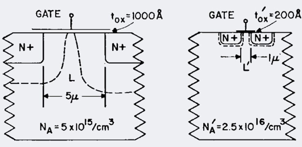 Image: IEEE
October 1974
Robert H. Dennard and colleagues at IBM describe how transistors can scale reliably to smaller dimensions, the essence of Moore’s Law. The Dennard scaling equations describe how to reduce all of the transistor’s major parameters, including the operating voltage, capacitance, and power, as the transistors become smaller. The guidelines run out of steam only when the operating voltage can no longer be reduced as quickly as required. Dennard says the equations provide “the physical foundation that enabled the realization of Gordon Moore’s observations.”
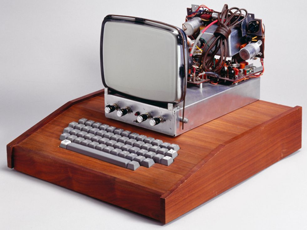 Photo: SSPL/Getty Images
June 1975
Stephen Wozniak finishes designing the predecessor of the
Apple I personal computer, offering 4 kilobytes of DRAM. “Woz” soon joins with friend Steven Jobs, forming Apple Computer in April 1976. The duo improves on the initial design by adding a faster microprocessor and more DRAM. Apple’s sales jump from $7.8 million in 1978 to $117 million in 1980. The first personal computers sell surprisingly well, propelling chip demand and spurring higher levels of integration on chips.
 Photo: Imec
April 1976
Japan’s Very Large Scale Integrated (VLSI) Semiconductor Project is established. It demonstrates that researchers from competing companies can cooperate to solve chip manufacturing challenges and share R&D costs, which are increasingly beyond the resources of any one company. Five Japanese semiconductor manufacturers form the project’s core, which receives 70 billion yen (approximately US $280 million) in public funding over five years. In response, the U.S. semiconductor industry forms the Semiconductor Research Corp. (SRC) in 1981. In 1988, Sematech sets up shop in Austin, Texas, with Robert Noyce as its first CEO. Three years later, Europe’s research consortium, Imec [above], begins fostering precompetitive R&D in Leuven, Belgium.
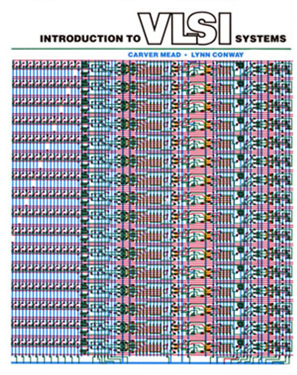 Photo: Addison-Wesley Pub
August 1977
Carver Mead, with Lynn Conway, begins writing his landmark book, Introduction to VLSI Systems, publishing it the following year. The book heralds a revolution in chip design, in which computer aided design (CAD) replaces the time-consuming custom design and hand-crafted layout of circuits. Mead, David L. Johannsen, and Edmund K. Cheng establish Silicon Compilers Inc. (SCI) in 1981; from 1983 to 1984, the team designs, in seven months, a key chip used in Digital Equipment Corp.’s MicroVAX minicomputer. The success of these automated design techniques sets the stage for the fabless semiconductor industry: Using design tools based on Mead’s insights, companies focused on semiconductor design begin cooperating with companies specializing in chip manufacturing—foundries—which produce chips for customers on a contract basis.
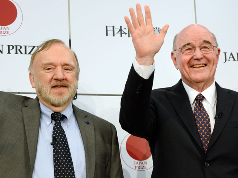 Photo: Toru Yamanaka/AFP/Getty Images
June 1982
IBM researchers C. Grant Willson
[above, right], Hiroshi Ito, and Jean M.J. Fréchet [above, left] describe a method of using new chemical compounds to increase the sensitivity to light of the photoresists used to pattern silicon wafers during chipmaking. These “chemically amplified” photoresists prove to be far more sensitive to the ultraviolet light used in lithography, speeding up the patterning process. IBM first introduces them for DRAM production in 1986.
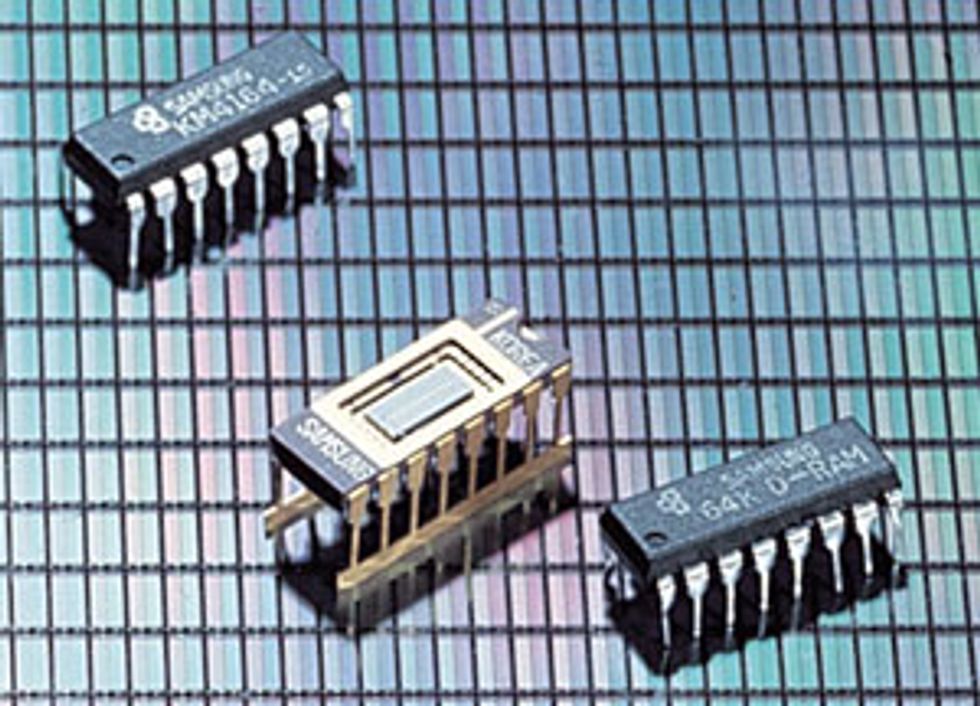 Photo: Samsung Electronics Corp.
September 1982
Engineers work around the clock at Samsung Electronics Corp. to finish designing the company’s first 64-kilobit DRAM. Hyundai Electronics Co. and LG Electronics follow suit, and the three companies quickly establish South Korea as a
major hub of the semiconductor industry. By 1994 Samsung becomes the leading producer of both 1-megabit and 4-Mb DRAMs, and in 2002 it becomes the No. 2 chipmaker, behind Intel, in worldwide revenues from semiconductors.
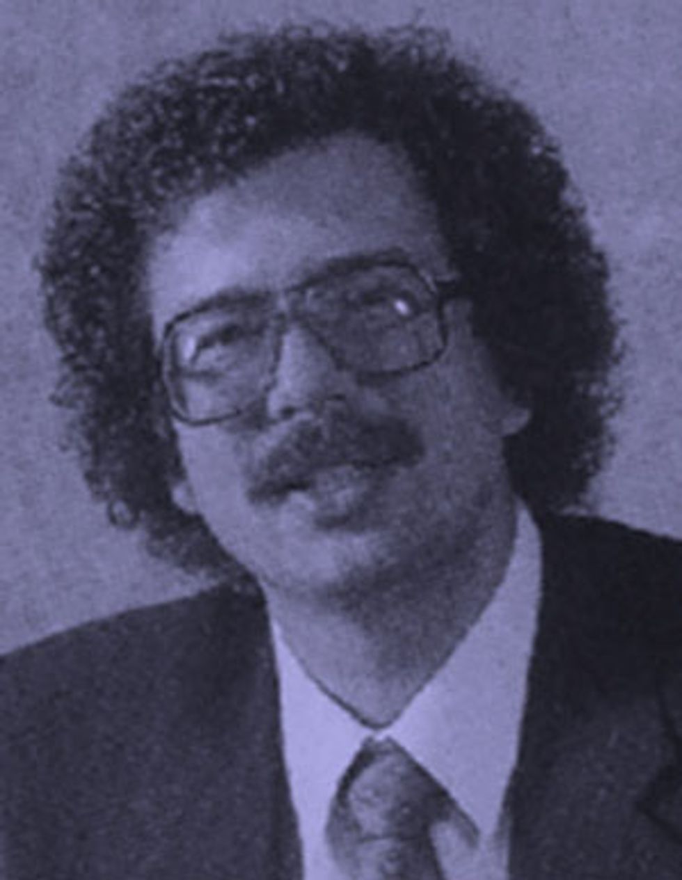 Photo: Xilinx
March 1984
Ross H. Freeman, a cofounder of Xilinx,
develops a field programmable gate array (FPGA) based on a static random-access memory (SRAM) cell. Freeman, who died in 1989, postulates that because of Moore's Law, transistors would be getting less expensive each year, making customizable, programmable chips affordable. His prediction is proved true, as engineers increasingly turn to FPGAs to try out ideas for a circuit without having to design and fabricate an application-specific integrated circuit, or ASIC. FPGAs also allow companies to remotely upgrade the software in equipment in the field.
 Photos: Fujio Masuoka (2)
December 1984
Flash memory, a new kind of electrically erasable and programmable read-only memory (EEPROM), is announced at the International Electron Devices Meeting. At the meeting, Fujio Masuoka describes what is now called NOR flash. A few years later, at the 1987 IEDM, Masuoka describes the serial NAND flash. Chipmakers go all out to increase the capacity of NAND flash memories, reaching gigabit densities on a single chip by 2002.
1985
Chipmakers start wider use of metallic compounds called
silicides to reduce the resistance in key areas of transistors on chips. Silicides, such as titanium disilicide for logic circuits, are added to a substance called doped polysilicon to link transistors. The metallic silicides provide lower-resistance gates and source-drain connections, greatly speeding up circuits. The first silicide in memory chips, tungsten, reduces the resistivity by an order of magnitude. Since then, semiconductor makers have turned to silicides including cobalt, nickel, and platinum, overcoming a series of tricky heat-related challenges to make them work.
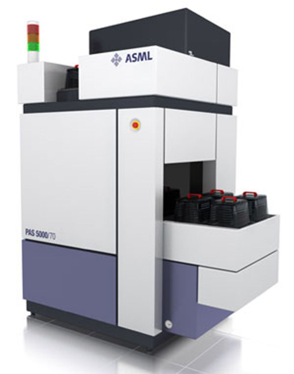 Photo: ASML
1985
GCA Corp. develops, for Bell Labs, deep-ultraviolet (DUV) equipment for making chips. The equipment, a stepper, uses 248-nm-wavelength laser radiation. It’s a big leap for lithography, as DUV laser light sources enable scanners to print much smaller features and much more quickly than mercury-lamp-based scanners. The lithographic advances build on the invention of the excimer laser in 1970 by researchers at the Lebedev Physical Institute. The GCA stepper uses a laser that generates photons from krypton fluoride gas. In 1990, SVG Lithography, with backing by Sematech, introduces the first DUV step-and-scan tool. It combines features of steppers and scanners, which were competing techniques for exposing wafers. ASML, which would eventually dominate the step-and-scan market, ships its first KrF (248-nm) stepper
[above] in 1991.
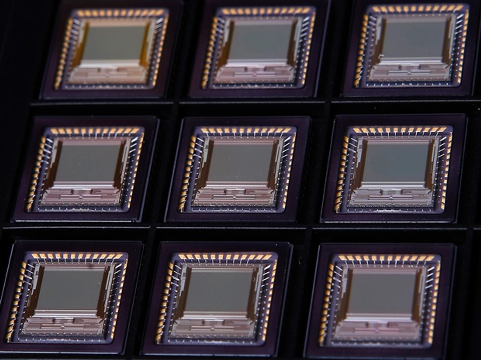 Photo: Corbis
December 1985
In an interview with
Computerworld magazine, spokesman Andy Roth of Advanced Micro Devices says: “Obviously the trend toward CMOS will continue until it becomes the dominant technology in the industry.” In the 1980s, p-channel metal oxide semiconductor (PMOS) and n-channel metal oxide semiconductor (NMOS) technologies are largely eclipsed by complementary metal oxide semiconductor (CMOS) technology, which combines the two to make superior circuits. By the mid-1980s, U.S.- and Japan-based companies are producing CMOS DRAMs in high volumes. Japanese companies then ride the demand for DRAMs and static RAMs made with CMOS to a dominant position in the semiconductor market. The breakthroughs that made CMOS viable were transistor gates that during fabrication could be self-aligned over the channels of the transistors and were made of polycrystalline silicon (“polysilicon”). MOS transistors soon begin displacing bipolar devices, another kind of semiconductor technology, largely because of CMOS’s lower power consumption.
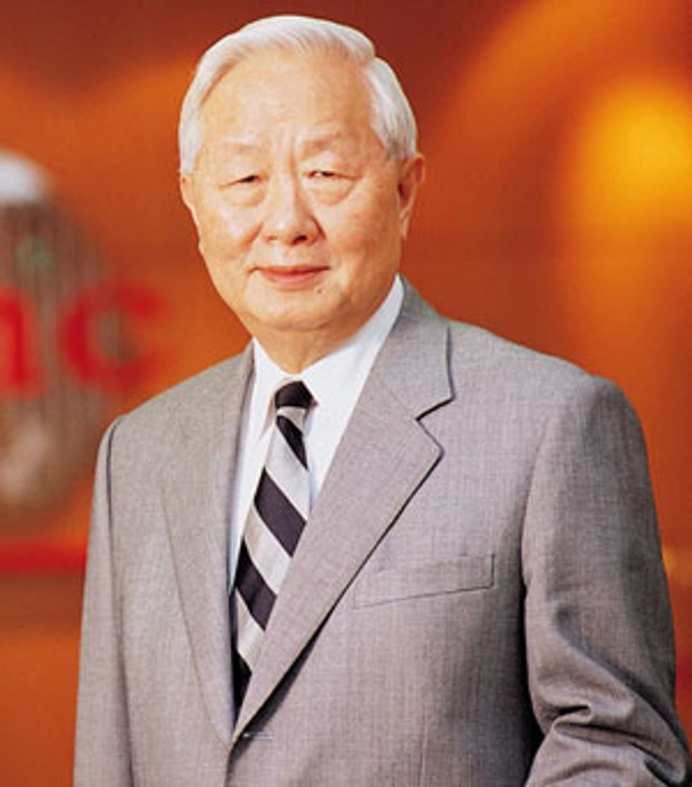 Photo: ASML
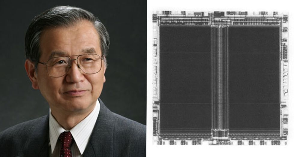
February 1987
With financial backing from Philips and the Taiwan government, ex–Texas Instruments executive Morris Chang starts
Taiwan Semiconductor Manufacturing Co. TSMC introduces the pure foundry model: a “fab for hire,” making custom chips under contract for anyone who will pay for them. This model soon transforms the semiconductor industry. In 1994 UMC (United Microelectronics Corp.), also in Taiwan, begins its transformation from an integrated device manufacturer to a foundry; it becomes the second largest foundry, behind TSMC. The role of electronic design automation (EDA) in the growth of foundries proves critical. Foundries describe their fabrication processes, handing that information over to the EDA industry to develop libraries and design tools targeted to the foundries’ technologies. Thus foundries create huge opportunities for design teams without fabrication facilities, which cost billions of dollars.
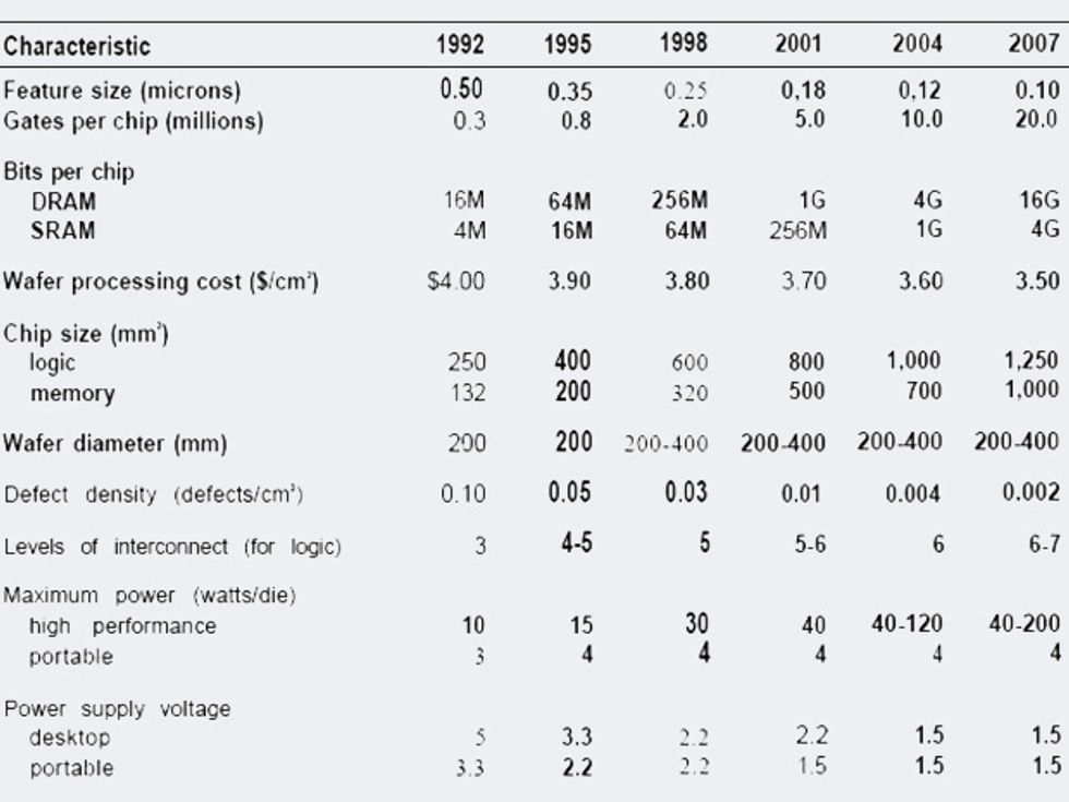 Image: Semiconductor Industry Association
November 1992
In the United States, the
Semiconductor Industry Association leads an effort that results in the first semiconductor road map, which is called the National Technology Roadmap for Semiconductors. It assumes a two-year period for the Moore’s Law doubling of transistors on chips and establishes goals for suppliers in all aspects of the chip industry. Using a color-coded scheme, the road map flags “red brick” challenges for which “no known solutions” are readily available. In 1999 the road map adds non-U.S. companies and becomes the International Technology Roadmap for Semiconductors, or ITRS.
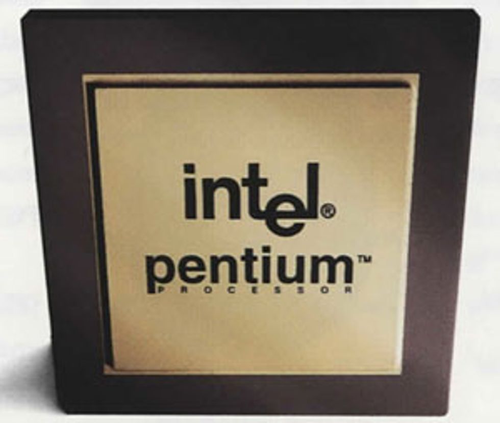 Photo: Intel
March 1993
Intel introduces
chemical-mechanical polishing (CMP), or planarization, as part of the interconnect-formation process in its Pentium processor. CMP, long used to polish optical lenses, had been thought too “dirty” to be included in high-precision fabrication processes, because abrasion tends to create particles that would interfere with projection lithography. But in the early 1990s, Japanese engineers use CMP to make the shallow trenches required to electrically isolate one transistor from another transistor. IBM develops CMP as part of its program to use copper, rather than aluminum for the metal connectors between transistors. The copper is deposited in trenches using electroplating, rather than sputtering-deposition methods.
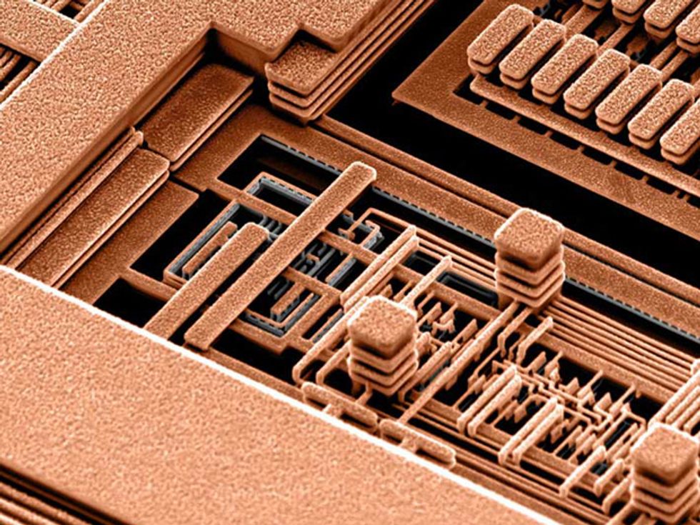 Photo: IBM
December 1997
IBM and Motorola introduce
copper interconnect technologies at the IEEE International Electron Devices Meeting (IEDM) in Washington, D.C. Intel, citing yield and cost concerns, waits until 2002 before abandoning the industry mainstay, aluminum, to connect one transistor with another. When a Wall Street Journal story on IBM’s work appears during IEDM, IBM’s stock price shoots up. Could it be that Wall Street pays attention to the importance of resistance-capacitance (RC) delays?
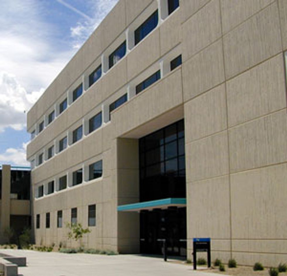 Photo: Intel
October 2002
Intel opens its first 300-millimeter high-volume wafer fabrication facility, called
11X, in Rio Rancho, N.M. The transition to the 300-mm (12-inch) diameter silicon wafers, from 200 mm, allows more than twice as many chips to be processed on a single wafer. The shift comes after several years of cooperative research and development within the 13-member I300I consortium, organized by the U.S.-based Sematech and Japan’s SELETE consortium.
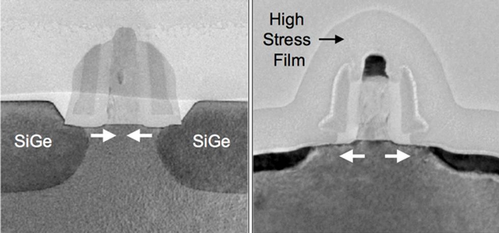 Image: Intel
December 2002
Intel introduces a new kind of material, called
uniaxial strained silicon, to its 90-nm transistors. The approach uses atoms, such as germanium, that are slightly larger than silicon atoms to add tension, or strain, within the silicon channel. The approach strains the silicon crystalline lattice in the direction orthogonal to the gate, boosting the speed of the electrons and holes as they zip through the silicon channel. Intel claims that strained silicon increases transistor performance by between 10 and 25 percent. The development heralds a shift, in which performance advances in chips start coming gradually but increasingly from new materials, such as silicon germanium and high-k and low-k dielectrics, rather than from the decreasing physical dimensions of the transistors themselves.
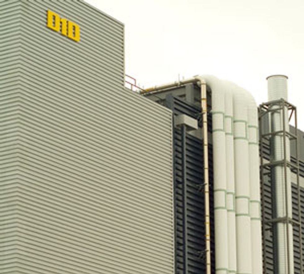 Photo: Bruce Forster
September 2003
Intel opens its
D1D fab facility in Hillsboro, Ore. The D1D, a development-production facility, is one of the first of a new generation of highly automated semiconductor manufacturing plants. The fab was constructed during an industry downturn that delayed the transition to factories processing 300-mm-diameter wafers; that delay allowed the semiconductor industry to introduce more-automated production techniques. Previously, technicians moved cassettes containing wafers being processed around by hand or in moving transport vehicles. But with the D1D, the industry switched to automated material handling systems. The cassettes are moved in overhead carriers that run in tracks placed in the ceiling of the 300-mm fabs. In a related development, producers of chipmaking equipment adopt a single standard for equipment control, referred to as single-wire control. Other standards, such as the standard mechanical interface (SMIF) allowed wafers to move into production equipment without being exposed to contamination.
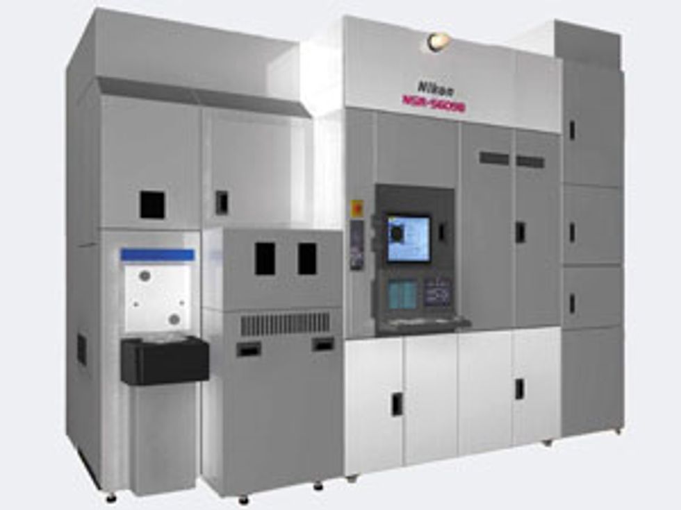 Photo: Nikon
February 2004
Nikon announces it has developed, and will market, an optical system for chipmaking based on immersion lithography. With scanners stuck at the 193-nm wavelength generated by argon-fluoride excimer lasers, the chip industry needs a new way to shrink critical dimensions of transistors. The answer: water. To shrink these dimensions requires a higher numerical aperture of the optical system. Because of its relatively high refractive index compared with that of air, a thin layer of water between the lens and the wafer enables optical specialists to increase—or widen the angle of—the aperture. This immersion lithography allows step-and-scan systems with a numerical aperture greater than 1.0, known as hypernumerical aperture steppers. Immersion, together with such exotic advances as phase-shift masks, off-axis illumination, within-tool alignment metrology, and optical-proximity correction, allows 193-nm scanners from ASML and Nikon to print critical dimensions a full order of magnitude smaller than the wavelength of the radiation used to project the patterns of the circuits on the chip.
 Photo: Tony Avelar/AFP/Getty Images
June 2007
Apple ships the first
iPhones, marking a transition from phones used primarily for telephone conversations to mobile devices used for data-centric applications such as Web surfing, e-mail, and later, texting. Smartphones from Apple, Motorola, Nokia, Samsung, and others soon drive higher and higher levels of integration on NAND flash chips and push chip-industry revenues to new heights. ARM Holdings provides low-power processor cores for many of the phones and tablets. Driven by the demands of mobile systems, higher performance per watt, rather than raw performance, becomes the industry’s goal for the first time.
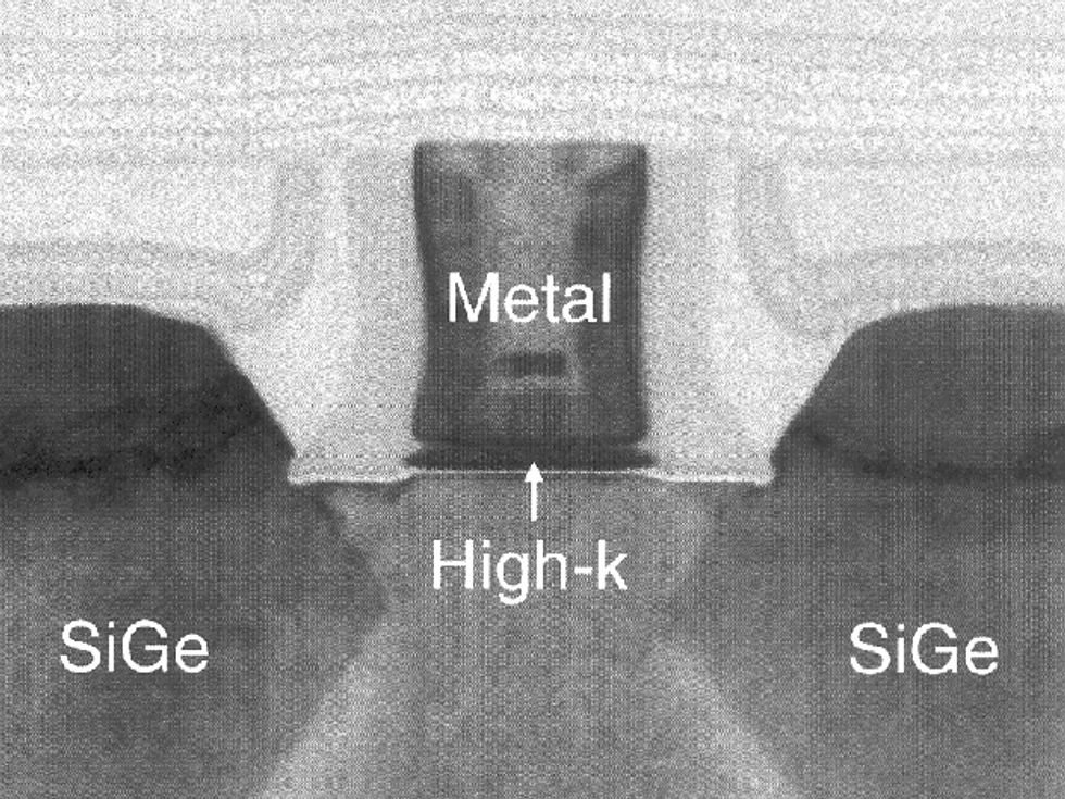 Image: Intel
December 2007
At IEDM, Intel announces that it has introduced a new insulating material into the transistors of its 45-nm technology generation. The
higher dielectric (high-k) material, based on a hafnium oxide compound, replaces silicon dioxide (SiO2) as the insulator of the transistors’ gates. The high-k layer prevents nearly all current from leaking through the controlling gate above the channel. Because of its electrical properties, the hafnium oxide layer allows the transistor to switch faster than SiO2-based gate materials. The transition comes after a long and painful search for a suitable material to succeed silicon dioxide. Sematech and Imec cooperate in narrowing down the material choices.
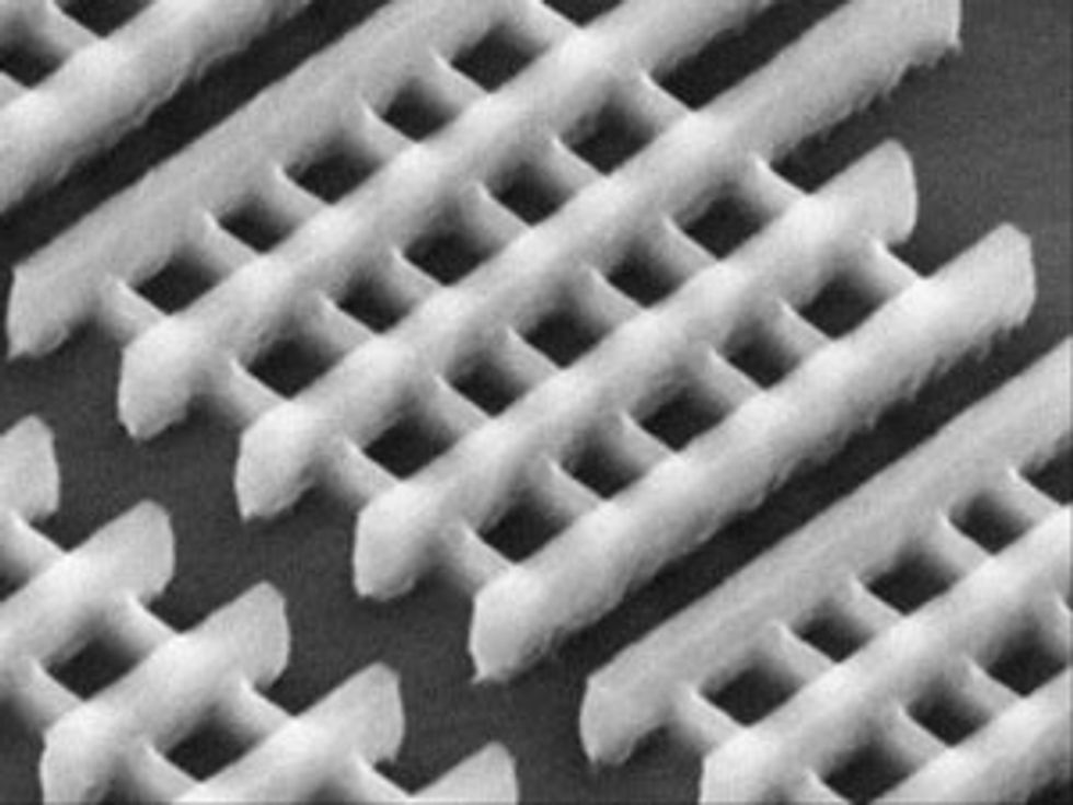 Image: Intel
May 2011
Intel senior fellow Mark Bohr discloses that the company has created chips containing a vertical transistor structure.
Chenming Hu of the University of California, Berkeley, and others had proposed a decade earlier that wrapping the transistor’s control gate around a tall, vertical channel would allow better switching compared with the horizontal approach. Intel surprises many observers by switching to a vertical, FinFET transistor earlier than expected, at the company’s 22-nm technology generation. The move to a vertical transistor represents a historic departure and requires solutions to a sobering series of lithography, etch, and other manufacturing challenges.
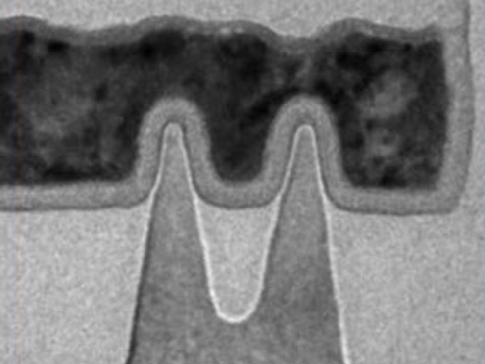 Image: Intel
December 2014
Gordon Moore’s prediction of component density doubling every two years appears to be holding, amazingly, after 50 years. At the 2014 IEDM,
Intel, IBM, TSMC, and Samsung present their FinFET transistor technology, based on a vertical channel and a control gate that wraps around the channel. The term “FinFET” derives from the finlike appearance of the channel. It allows the number of transistors for a given area to double compared with that for the previous generation.
Editor's note: The entry for June 2007 was corrected on 4 May 2015 to say “higher performance per watt” instead of “lower performance per watt.”
About the Author
David Lammers is a journalist based in Austin, Texas. He would like to thank the following people for their help with this timeline: Dave Gross of GlobalFoundries, Dan Hutcheson at the Chip History Center, Chris Mack of the University of Texas at Austin, Koji Sakui at Micron Japan, and An Steegen at Imec.
From Your Site Articles
{"imageShortcodeIds":[]}


