Want more computing power in your processor? Add more silicon. But complexity and cost are starting to erode that maxim.
“The absolute die size has been going up relentlessly over time and is trending to bump into” the limit of what chipmaking equipment can produce, Samuel Naffziger of Advanced Micro Devices (AMD) told engineers at the International Solid-State Circuits Conference (ISSCC) in San Francisco earlier this year. At the same time, for a fixed die size, the cost per square millimeter “has been increasing relentlessly and is now accelerating,” he says.
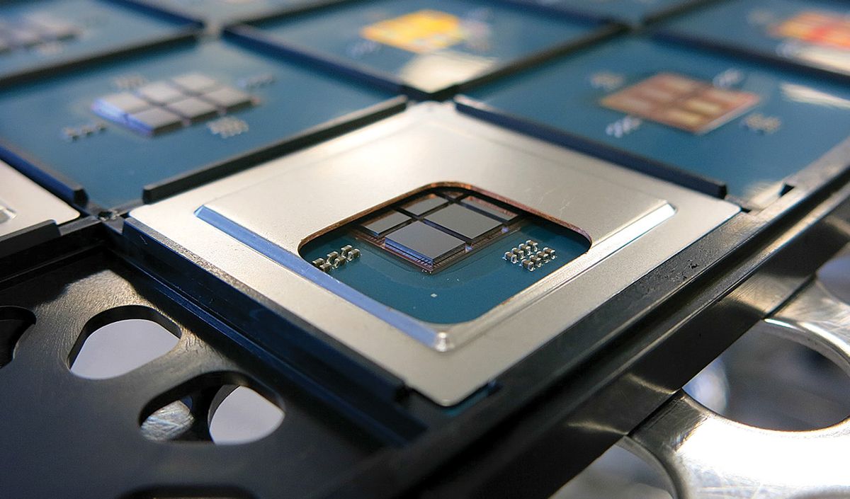
The combined squeeze of rising costs and ever-larger chip sizes is leading to a solution in which processors are made up of collections of smaller, less-expensive-to-produce chiplets bound together by high-bandwidth connections within a single package. At ISSCC, AMD, Intel, and the French research organization CEA-Leti showed how far this scheme can go.
The CEA-Leti processor stacks six 16-core chiplets on top of an “active interposer,” made of a thin sliver of silicon, to create a 96-core processor. The interposer houses voltage-regulation systems that are usually found on the processor itself. It also features a network-on-chip that uses three different communication circuits to link the cores’ on-chip SRAM memories. The network is capable of slinging 3 terabytes per second per square millimeter of silicon with a latency of just 0.6 nanosecond per millimeter.
Active interposers are the best way forward for chiplet technology, if it’s ever going to allow the integration of disparate technologies from multiple vendors into single systems, according to Pascal Vivet, a scientific director at CEA-Leti. “If you want to integrate chiplets from vendor A with chiplets from vendor B, and their interfaces are not compatible, you need a way to glue them together,” he says. “And the only way to glue them together is with active circuits in the interposer.”
Chiplet enthusiasts imagine a remaking of the system-on-chip industry so that chiplets from multiple vendors could all be integrated with little effort, thanks to standardized interfaces. The result would be cheaper, more flexible mix-and-match systems.
But industry is not there yet. Rather than produce simple mix-and-match systems, Intel and AMD each designed their new chiplets to coordinate closely with one another and with the packages that integrate them. Nevertheless, the results seem worthwhile.
Intel used its 3D chiplet-integration tech, called Foveros, to produce the new Lakefield mobile processor. Foveros provides high-data-rate interconnects between chiplets by stacking them atop one another and delivering power and data from the package vertically through the bottom die. At ISSCC, Intel’s Wilfred Gomes explained that among the goals for Lakefield was to boost graphics computation by about 50 percent while consuming one-tenth the standby power of its predecessor. No single manufacturing process can produce transistors that would achieve both targets, but Foveros allows for mixing dies that have transistors designed for high-performance computing with those designed for superior standby power consumption.
AMD has been using chiplets connected on an organic substrate within the chip package. At ISSCC, the company detailed how it designed the chiplets and package together for its second-generation EPYC high-performance processors. The previous generation had been made up of four chiplets. But in order to fit more silicon in while keeping costs down, the company redesigned the chiplets so that only the computing cores were upgraded to Taiwan Semiconductor Manufacturing Co.’s 7-nanometer process technology, the most advanced available. All other functions were piled into a central input/output chiplet made using older, less costly technology. Once that was done, “we had to figure out how to route nine chiplets in the same package size that we had done with four,” said Naffziger. The result was “an unprecedented amount of silicon/package codesign.”
This article appears in the May 2020 print issue as “Chiplets Are the Future of Processors.”
Samuel K. Moore is the senior editor at IEEE Spectrum in charge of semiconductors coverage. An IEEE member, he has a bachelor's degree in biomedical engineering from Brown University and a master's degree in journalism from New York University.


