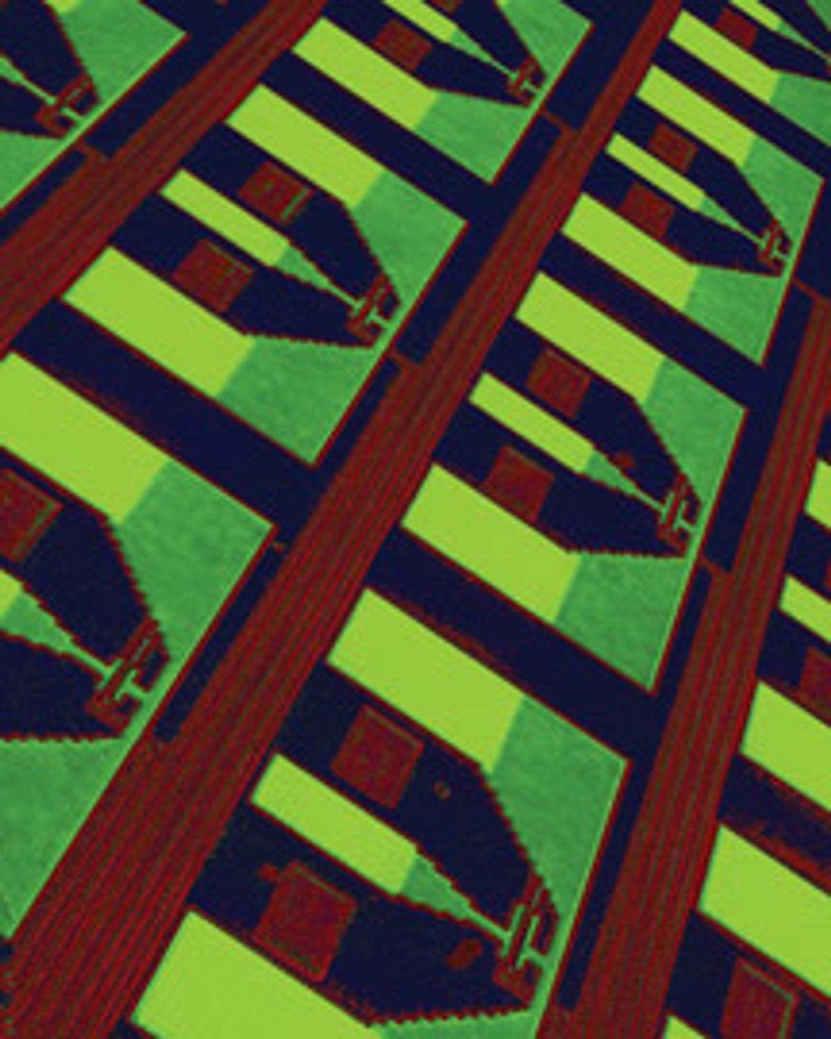
A better photodetector could bring optical data transfer between computer chips closer to reality, according to the IBM researchers who created the device. Such an advance could overcome a looming speed limit—the rate at which data can move between a processor’s cores, or from one chip to another, over copper wire.
The detector is built from a germanium crystal that amplifies signals tenfold, operates at 40 gigabits per second, and consumes one-twentieth the power of previous efforts while producing less noise. Solomon Assefa and his colleagues at IBM’s T.J. Watson Research Center, in Yorktown Heights, N.Y., reported on their work in the 4 March issue of Nature.
”The idea is to build all the different components we need to replace copper wires,” Assefa says. The photodetector ”was basically the last piece of the puzzle.” Niche applications for the detectors may come soon, he adds, but it may be as long as 10 years before they can be used in high-end computing.
Germanium is attractive because it’s compatible with silicon and is already used in complementary-metal-oxide semiconductor manufacturing. But a germanium avalanche photodiode, which amplifies a signal by using an incoming photon to create a cascade of electrons, produces too much noise to differentiate the signal. In 2008, Intel came up with a solution that used a layer of germanium to detect the photons and a layer of silicon to do the amplification, but the sheer size of the device, about a micrometer thick, limited signal speed to about 10 Gb/s.
The IBM team overcame the limits of germanium by controlling the characteristics of electric fields in the device over a distance of just a few nanometers. They placed a series of tungsten plugs in a thin layer of germanium and attached lines of copper to the plugs. The close spacing of the plugs, 200 nanometers apart, combined with the thinness of the germanium, 150 nm thick, created very strong electrical fields in the germanium, which sped up the electrons. It also narrowed the range of energies of the charge carriers—both electrons and holes—which reduced the noise by as much as 70 percent.
Generally engineers deposit germanium on silicon through epitaxy, but because the two elements have different crystalline structures, strain between the materials causes defects. The IBM group used a rapid-melting growth technique instead.
The researchers started with a strip of silicon that would later act as a waveguide. On top of that they deposited a thin layer of silicon oxynitride that would isolate the silicon from the germanium so that the charge carriers wouldn’t pass between them in the finished device. They made a tiny hole in the oxynitride to expose a bit of the underlying silicon, then put down a thin layer of germanium on top to match the waveguide underneath. After adding another layer of oxynitride to encapsulate the germanium, they then heated the whole thing up until the germanium melted. Because the germanium was touching the still-unmelted silicon through the hole, as it cooled, the silicon acted as a crystalline seed, imprinting its structure onto the germanium, which formed a single crystal.
These are the first detectors that can amplify the input tenfold and work at 40 Gb/s, ”which will be extremely important for on-chip interconnects,” says Franz Kaertner, an electrical engineer at MIT, who was not involved in the project. Though integrated germanium photodetectors have been demonstrated before, none performed the amplification in the germanium layer itself, and none operated at such low voltage. ”In that context it is unique,” he says. The challenge now, he adds, is to reduce the current that runs through the device in the absence of an input of light, a type of noise called dark current.
About the Author
Neil Savage writes about technology from Lowell, Mass. In March 2010, he reported on ways to reduce the radiation used in medical scanners.

