
Sad but true: About three-quarters of the time, your computer processor is doing nothing more than waiting for data—the cybernetic equivalent of twiddling one’s thumbs. It doesn’t matter whether you’ve got the latest processor, surrounded it with high-speed RAM, or lovingly hot-rodded your system with the latest in liquid cooling. Your speed is primarily set not by the processing power you have but by the connections that stand between that processor and the data it needs.
The problem is that data transfer is accomplished by the movement of an electronic signal along old-fashioned copper wires—the same basic phenomenon that a century and a half ago carried news of the U.S. Civil War over telegraph lines. It’s time we saw the light—literally—and stopped shackling ourselves to electrons moving along copper conductors.
For decades, engineers have sought to transfer signals from chip to chip with photons. Photons are more than just fast; unlike electrons, they lack an electric charge. That means they can’t interfere with each other, causing cross talk that, like the din of a boisterous party, can turn a conversation into a game of charades. For many years, however, the optoelectronic strategy has been hindered by the problem of getting photons to go where you want them to go. Metal connections can be laid down on semiconductor wafers with exquisite precision, and they can easily be formed into networks that branch out from central lines, the same way capillaries branch out from arteries. It’s far harder to accomplish this feat when laying down a system of tiny optical channels.
At IBM, we have now developed a first-of-its-kind optical data-transfer system, or bus, built right onto the circuit board. With it, we will soon unveil computer systems 100 times as fast as anything available today. With that much muscle, scientists will at last be able to visualize wondrous things in detail: how the climate will react to man-made greenhouse gases, how neurons organize to form a brain, how to custom design a drug to treat an individual patient.
Ever since the early days of microprocessors, data has shot back and forth far faster inside the chip than between the chip and external components, such as memory and input/output ports. Data transfers within a microprocessor—for example, between the processing core and on-chip cache memories—have been operating at multigigahertz clock rates for more than a decade. But transfers between the chip and external memories along those copper conduits are typically an order of magnitude slower. This bandwidth gap will continue to widen as processor performance continues to climb and multicore architectures become more elaborate.
Copper can’t keep up, because it faces simple physical limits. Shoot an oscillating signal down a long copper line on a printed circuit board and it’ll lose about half its strength at 2 gigahertz—and a staggering 98 percent at 10 GHz. Most of that loss stems from two effects. First, the oscillating signal induces stray currents in the board’s conductors that suck away energy. Second, induced currents inside the wire itself push electrons to the surface of the metal, reducing the effective cross section of the wire and thus raising resistance. The higher the frequency—that is, the clock rate—of the signal, the greater the losses will be.
To make matters worse, severe resonances occur at a few gigahertz, at which point the signal begins to reflect off metal paths in the vias, the vertical conductors that connect elements of a circuit board. It gets worse still as bit rates approach 10 gigabits per second, when cross talk blurs the signal, even at distances of less than a meter.
These problems are particularly bad when you’re yoking together the multichip modules of a massively parallel computer. When one module must link up with another at the other end of a circuit board or, worse still, in a different rack of equipment, the bandwidth bottleneck becomes particularly severe. That’s why today’s highly parallel machines can reach peak performance only when solving those specialized problems that can be readily divided into many tasks that can be processed independently.
By avoiding all those signal-loss and cross-talk problems, an optical bus would make supercomputers go much faster. It would also make them easier to program, because programmers wouldn’t have to take special measures to compensate for such severe communication delays among processors.
Fiber-optic lines first began proliferating in the 1980s in long-distance telecom networks. By the late 1990s, fiber-optic links had found their way into local and storage area networks, interconnecting systems hundreds of meters apart. Over the next decade, the technology kept moving down to ever smaller dimensions as its cost and power needs kept falling and the bandwidth requirements of computer systems kept rising.
Consider the role of optical interconnects in supercomputing. In 2003 and 2004, the fastest machines on Earth were the NEC Earth Simulator and IBM’s initial Blue Gene L, which had peak performances of around 36 trillion floating-point operations per second, or teraflops. All the interconnects in those supercomputers were electrical. Then, in 2008, IBM’s Roadrunner set a new record by achieving a quadrillion (a thousand million million) such operations per second, which is known as a petaflop. The Roadrunner used some 40 000 optical links to connect entire racks of servers.
Sometime next year, at the National Center for Supercomputing Applications at the University of Illinois at Urbana-Champaign, IBM’s Blue Waters machine is expected to go 10 times as fast, using more than 1 million optical interconnects. The number of parallel optical modules inside Blue Waters will be roughly equal to the world’s current annual production. IBM will be a major consumer of these optical interconnects, and though it helped to pioneer parallel optics, IBM does not plan to go into the business of manufacturing the modules. So the company is sharing much of its knowledge with potential suppliers.
Computers beyond Blue Waters will need proportionately more interconnects. Connect the dots and the resulting trend suggests that 1000-petaflop (Pflop) systems will require an astonishing 400 million optical links. In general, judging from past performance data, supercomputer processing rates have been going up tenfold every four years. So you can expect 10-Pflop, 100-Pflop, and 1000-Pflop (exaflop) systems to emerge in 2012, 2016, and 2020, respectively. The Blue Waters system—starting at 10 Pflops, and scalable to 16 Pflops—is slightly ahead of the trend, with a scheduled production date of 2011.
To sustain this exponential performance increase, we’ll have to cram more optical links into a given space at lower cost and integrate those links more fully into the computer’s electronic processors. Since 2003, IBM has led a project, sponsored by the Defense Advanced Research Projects Agency, or DARPA, that aims to do just that, by bringing optical communications down to the level of the circuit board. This project, conducted at three of the company’s global research labs (Yorktown Heights, N.Y.; Zurich; and Tokyo), is developing optical transceivers mounted on and communicating through optically enabled printed circuit boards. The boards incorporate a layer of optical “wiring,” or buses, that can move data between processor modules.
The scale of the printed circuit cards and backplanes used in today’s supercomputers is about 10 to 200 centimeters. For optical buses to compete with copper interconnects at this scale, the performance and efficiency of optics must become much better than they are. Optical modules with 12 parallel channels now cost several dollars per gigabit per second, offer speeds from 60 to 120 Gb/s with an efficiency of 30 to 100 picojoules per bit, and occupy about two-thirds of a square centimeter on the chip. To be practical for 100-Pflop machines, these modules must be improved on all fronts by a factor of 10 and will have to be scaled commensurately beyond that for exaflop computers.
To scale up the modules, we’ll have to stop using a separate optical fiber to link each transmitter with its corresponding receiver. That makes for a heck of a wiring job, now that the number of optical links in a supercomputer already exceeds 1 million. Just imagine the tangled confusion on a PC motherboard if every electrical bus were constructed with individual wires instead of traces in a multilevel printed circuit board! It would be impossible to build.
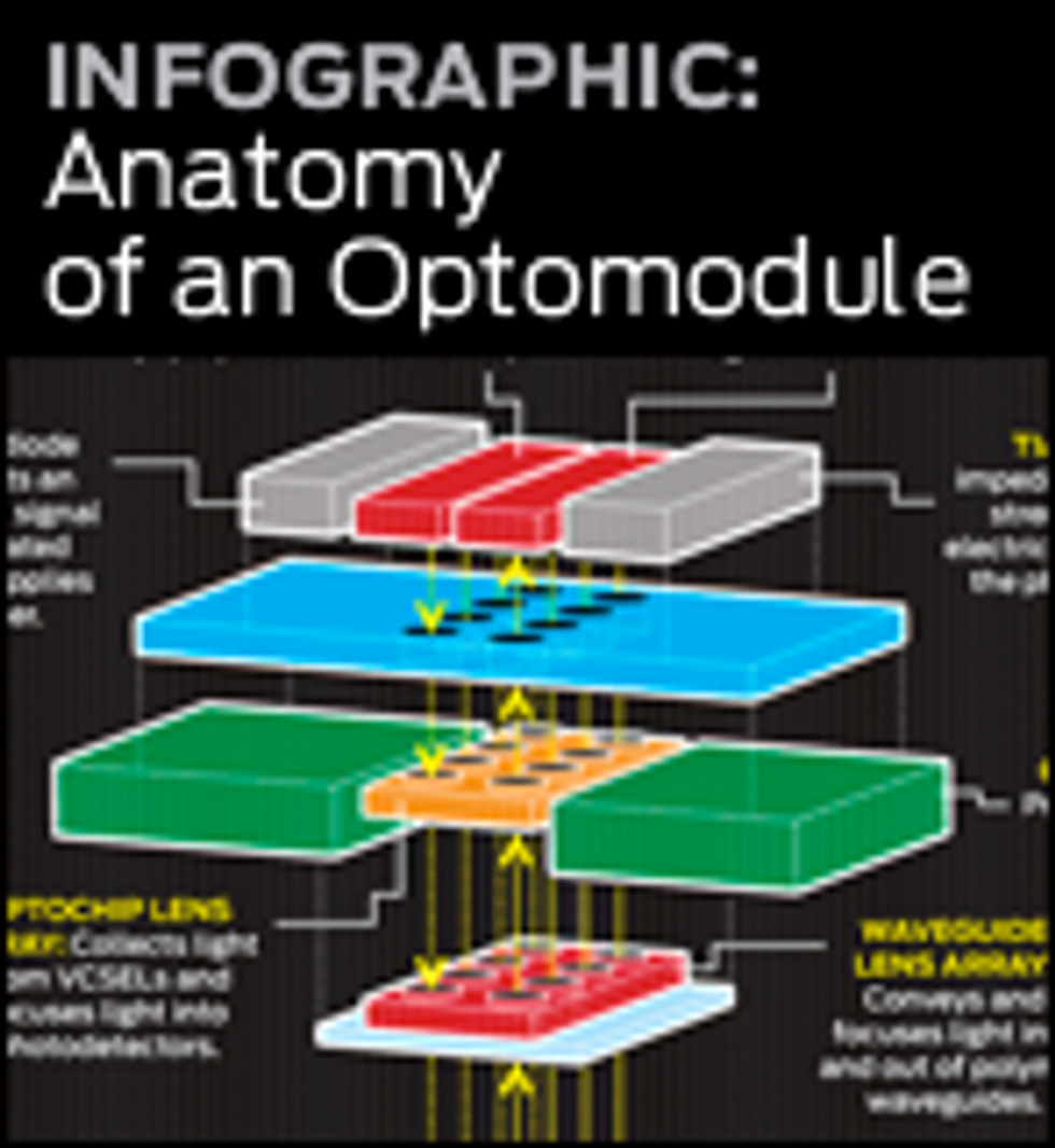
We are developing parallel optical devices that will soon have the kind of speed, density, and cost profile we are seeking. We call them optochips. Optochips are transceivers: They convert signals from electrical to optical form and back again. They simultaneously transmit and receive optical data through many dozens of communication channels—a number that may rise to hundreds in the future—to achieve a huge aggregate bandwidth. And they are similar enough to standard electronic chips to be packaged and installed using conventional, low-cost assembly techniques, such as surface mounting on a circuit board.
We have built two quite different optochips, one operating on optical signals at 985 nanometers and the other at 850 nm. They both use vertical-cavity surface-emitting lasers (VCSELs) as the light source. These lasers can be modulated at speeds of up to 40 Gb/s, and they emit light vertically through mirrors, along a path perpendicular to the chip. The lasers are particularly inexpensive to manufacture, in part because they are fabricated in two-dimensional arrays and so can be tested right on the wafer, before it has gone through further processing steps. (VCSELs are so inexpensive—just pennies per device—that they’re now found in nearly all optical mice.) The first commercial parallel modules employing VCSELs appeared in the late 1990s and operated at about 1 Gb/s per channel, but the market started to take off only around 2003, when such interconnects began to link racks in computers and routers. The data rates quickly rose, recently reaching 10 Gb/s per channel.
We built the 985-nm optochip first. It has the simplest and most compact package because it takes advantage of a feature called substrate emission and detection. This enables the device to emit light downward, into the substrate—that is, in exactly the opposite direction from that of standard VCSELs. Similarly, the 985-nm optochips also receive light through the substrate. The light is detected by a photodiode integrated into the optochip.
By configuring the laser and photodiode detector this way, we can put their respective electrical contacts on one side, so they don’t obscure the window for transmission. We can also put lenses that collimate the beam on the bottom, so we’re able to pack lenses in more densely. Also, because light goes in and comes out through the back surface of the optochip, the front side of these chips can be directly soldered to a single CMOS transceiver chip. This chip converts the optical signals to electrical ones, and vice versa. The chip is fabricated with a low-cost, 0.13-micrometer process and measures just 3.25 by 5.25 millimeters. It contains the circuits that amplify the signals that go into the laser and those that come out of the photodetector.
We soldered two 4-by-4 arrays of devices onto the CMOS transceiver chip, one of lasers and the other of photodetectors. Each 16-device array connects to 16 distinct amplifying circuits on the CMOS chip. This is a highly compact way to assemble this parallel design, and it could readily be scaled up to offer even more transmitter and receiver channels.
The optochip operates at up to 15 Gb/s per channel—the previous record was 10 Gb/s per channel. And all of its 16 channels together provide an aggregate bandwidth of 240 Gb/s while consuming just 2.2 watts of power.
Besides its blazing speed, the optochip can send and receive a single bit with a paltry 9 pJ, an efficiency that’s about five times that of the modules now on the market. It’s also able to transmit a lot of information per unit of area, achieving 28 Gb/s per square millimeter. That’s the highest bandwidth density achieved to date and at least 10 times that of the latest commercial parallel optics. Density is obviously critical in large systems: If you’re going to have 100 million optical links, they’d better be small.
The Terabus program began in 2003 as a joint effort between IBM and Agilent Research Laboratories, in Santa Clara, Calif. IBM was responsible for developing the waveguide, circuit board, CMOS design, and packaging, while Agilent produced the arrays of lasers and photodetectors. Then in 2005, Agilent spun out its semiconductor products division and withdrew from the program. Although we had enough of the critical 985-nm lasers and photodetectors to attain the initial program milestones, we decided to redesign the optical transceivers to incorporate 850-nm VCSELs and photodiodes.
By doing so, we had to give up substrate emission—the very feature that let us make our first-generation optochip so compact and elegant. The reason was that the substrates of the lasers and detectors aren’t transparent to 850-nm radiation (more on that in a moment). Nevertheless, with our new 850-nm optochips we were able to exploit a few countervailing advantages. First, the optical transceiver industry was producing 850-nm parts in high volumes; if we’d bet on another wavelength, we would have had to spend a lot of money on R&D to establish an industry standard. In fact, the 850-nm parts we now use are fabricated by Emcore Corp., in Albuquerque. They differ from Emcore’s standard parts mainly in offering 24 rather than 12 channels.
Second, there was a purely technical motive behind our selection of the 850-nm transceivers. Less light is lost in the polymer waveguides at 850 nm than at 985 nm. That loss matters, particularly at links of up to a meter long—the length we had resolved to support in our Terabus project. On that scale, by working at 850 nm instead of 985 nm you get a whopping six times as much optical power through to the receiver.
Because the substrates of the lasers and detectors are not transparent to 850 nm, we couldn’t solder them directly to the CMOS transceiver without blocking the path of the light. So we designed an additional simple silicon “chip” measuring 10.4 by 6.4 mm to serve as a carrier. The laser and photodiode arrays are soldered to it, along with two new 24-channel CMOS chips, one a transmitter and the other a receiver.
This silicon carrier chip (which has no transistors or other active devices) has three wiring levels on its upper surface, formed of alternating layers of copper and oxide insulation. Metal wires extending through the silicon connect these wiring layers through the chip to bonding pads on the opposite surface of the carrier. The top wiring connects each of the 24 optical devices to its own amplifier (either a laser driver or a receiver channel). To allow light to pass through the carrier, we etched holes—optical vias, that is—through the carrier below each laser and detector device.
Our 850-nm design gives us half again as many channels as the previous chip did—24 transmitters and 24 receivers, each operating at up to 15 Gb/s per channel. Together they achieve a bidirectional data rate of 360 Gb/s while consuming 2.3 W of power. The power efficiency, at 6.5 pJ per link, beats that of the 985-nm optochips, though the bandwidth density, at about 9 Gb/s/mm2, is only about a third as good. All in all, it’s a good bargain, because the 850-nm optochip was specifically designed to use only components that can be mass-produced at low cost, using lasers and photodetectors that are available today.
Exploiting this power requires that we raise the integration level to cover an entire circuit board. We therefore built a board-spanning optical bus by packaging optochips on a fabricated optical printed circuit board. We started by soldering optochips to chip carriers. This is the same type of electrical packaging that is used today for microprocessors in a laptop. A hole in the carrier provides a path for the light signals between the optochip and the circuit board, so the mirror can bend the light by 90 degrees.
Ours is the first optical data bus ever integrated into a printed circuit board. So far, we’ve been able to transfer data at 10 Gb/s along a 15-cm bus through 32 one-way links between two of our 985-nm optochips. We provided a dramatic illustration of this bus at the SC07 supercomputer trade show, in 2007. At that conference, one of our optochips transferred a video signal from an HDTV camera to a second optochip over a single waveguide channel and was displayed live on an HDTV monitor for more than three days. Although we used only a single channel, at a data rate of 2 Gb/s the card and optochips could support more than 160 simultaneous HD video signals.
Our transceiver technology clearly achieves bandwidth and power efficiencies way beyond the capabilities of anything on the market today. Can it go from the laboratory to high-volume manufacturing? We’re confident that it can: Our transceivers incorporate CMOS electronics, optoelectronic devices, and microchip packaging techniques that are already in production today. Product development should be straightforward.
Within five years, we hope to connect microprocessors and memory chips right to the optochip, producing the optical analogue to the electrical multichip modules in today’s big-iron machines. In these near-future supercomputers, electrical connections will supply only the power, the ground, and the control signals. All the data will shoot through optical interconnects at the speed of light.
About the Author
Clint Schow, Fuad Doany, and Jeffrey Kash work at the IBM T. J. Watson Research Center in Yorktown Heights, N.Y. Their mission is not to speed up processors but to deal with the shortage of bandwidth between them—an irksome problem that must be solved if future generations of supercomputers and servers are to be more powerful than today’s.